
Datasheet


MAX5322
±10V, Dual, 12-Bit, Serial, Voltage-Output DAC
16 ______________________________________________________________________________________
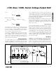
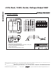
(max), DOUT is high impedance, and OUTA and OUTB
are pulled to SGNDA and SGNDB, respectively, through
the internal feedback resistors of the output amplifier
(Figure 1). When coming out of shutdown, or during
device power-up, allow 350µs for the output to stabilize.
Applications Information
Power Supplies
A single supply of +12V to +15V is required to realize an
output swing of 0 to 10V. A dual supply of ±12V to ±15V
is required to realize an output swing of ±10V, and allows
unipolar, 0 to +10V output if UNI/BIP_ is forced high. A
+3V to +5V digital power supply and two +2.000V to
+5.250V external reference voltages are also required.
Always bring up the reference voltages last; the other
power supplies do not require sequencing.
Power-Supply Bypassing and
Ground Management
Bypass V
DD
and V
SS
with 1.0µF and 0.1µF capacitors to
AGND, and bypass V
CC
with a 1.0µF and 0.1µF capaci-
tors to DGND. Minimize trace lengths to reduce induc-
tance. Digital and AC transient signals on AGND or
DGND can create noise at the output. Connect AGND
and DGND to the highest quality ground available. Use
proper grounding techniques, such as a multilayer board
with a low-inductance ground plane or star connect all
ground return paths back to AGND. Carefully lay out the
traces between channels to reduce AC cross coupling
and crosstalk. Wire-wrapped boards, sockets, and
breadboards are not recommended.
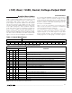
BINARY DAC CODE ANALOG OUTPUT
MSB LSB UNIPOLAR (UNI/BIP_ = HIGH) BIPOLAR (UNI/BIP_ = LOW)
1111 1111 1111 +2 x V
REF
(4095 / 4096) +2 x V
REF
(2047 / 2048)
1000 0000 0001 +2 x V
REF
(2049 / 4096) +2 x V
REF
(1 / 2048)
1000 0000 0000 +2 x V
REF
(2048 / 4096) = V
REF
0
0111 1111 1111 +2 x V
REF
(2047 / 4096) -2 x V
REF
(1 / 2048)
0000 0000 0001 +2 x V
REF
(1 / 4096) -2 x V
REF
(2047 / 2048)
0000 0000 0000 0 -2 x V
REF
(2048 / 2048) = -2 x V
REF
Table 3. Output Voltage as Input Code Examples
hex DIGITAL INPUT CODE (LSB)
-2048
-2047
-2046
-2045
+2047
+2046
+2045
+2044
+1
0
-1
ANALOG OUTPUT VOLTAGE (LSB)
001
000
002
003
7FF
800
801
FFC
FFD
FFF
FFE
4 x V
REF
1 LSB =
4 x V
REF
4096
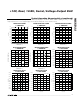
Figure 6. Bipolar Transfer Function
hex DIGITAL INPUT CODE (LSB)
0
1
2
3
4095
4094
4093
4092
2049
2048
2047
ANALOG OUTPUT VOLTAGE (LSB)
001
000
002
003
7FF
800
801
FFC
FFD
FFF
FFE
2 x V
REF
1 LSB =
2 x V
REF
4096
Figure 5. Unipolar Transfer Function