
Datasheet


where:
Bipolar output voltage:
where:
where V
OUT_UNI
is the unipolar output voltage, V
OUT_BIP
is the bipolar output voltage, LSB
UNI
is the unipolar LSB
step size, LSB
BIP
is the bipolar LSB step size, V
REF
is
the reference voltage, and CODE is the decimal equiva-
lent of the binary, 12-bit, DAC input code.
In either case, a 000hex input code produces the mini-
mum output (-2 x V
REF
for bipolar and zero for unipo-
lar), an 800hex input code produces the midscale
output (zero for bipolar and V
REF
for unipolar), and a
FFFhex input code produces the full-scale output (2 x
V
REF
for bipolar and unipolar).
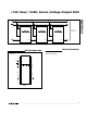
Output Amplifiers
The output-amplifier section can be configured as either
unipolar or bipolar by the UNI/BIP logic input. With
UNI/BIPA (UNI/BIPB) forced low, SW1 (SW4) and SW2
(SW5) in Figure 1 are closed, and SW3 (SW6) is open.
This configuration channels the DAC output through two
output stages to generate the ±2 x V
REF
output swing.
The first amplifier generates the ±V
REF
voltage range and
the second amplifier gains it up by two. When configured
for bipolar operation, the MAX5322 must be driven with
dual ±12V to ±15V power supplies.
With UNI/BIPA (UNI/BIPB) forced high, switches SW1
(SW4) and SW2 (SW5) are open and SW3 (SW6) is
closed. This configuration channels the DAC output
through only a single gain stage to generate a 0 to 2 x
V
REF
output swing.
Daisy-Chaining
SPI-/QSPI-/MICROWIRE-compatible devices can be
daisy-chained to reduce I/O lines from the host controller
(Figure 7). Daisy-chain devices by connecting the DOUT
of one device to the DIN of the next, and connect the
SCLK of all devices to a common clock. Data is shifted
out of DOUT 16.5 clock cycles after it is shifted into DIN,
and is available on the rising edge of the 17th clock
cycle. The SPI-/QSPI-/MICROWIRE-compatible serial
interface normally works at up to 10MHz, but must be
slowed to 6MHz if daisy-chaining. DOUT is high imped-
ance when CS is high.
Shutdown
Shutdown is controlled by software commands or by the
SHDN logic input. The SHDN logic input may be imple-
mented at any time. The SPI-/QSPI-/MICROWIRE-com-
patible serial interface remains fully functional, and the
device is programmable while shutdown. When shut
down, the MAX5322 supply current reduces to 2.8µA
LSB
V
BIP
REF
=
×4
2
12
V LSB CODE V
OUT BIP BIP REF_
( )( )=×−×2
LSB
V
UNI
REF
=
×2
2
12
MAX5322
±10V, Dual, 12-Bit, Serial, Voltage-Output DAC
______________________________________________________________________________________ 15
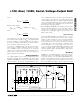
RRR
2R 2R 2R 2R2R
D0 D11D10D1
REFA
AGND
01010101
OUTA
CONTROL LOGIC
2R
2R
2R
2R
SGNDA
DAC REGISTER A
SW1
SW2
SW3
MAX5322
UNI/BIPA
Figure 4. Basic Inverted DAC Ladder