
Datasheet


MAX5322
and isolate the shift register from the DAC registers.
The DAC registers control the DAC ladder and thus the
output voltage. Any update to a DAC register updates
the respective output voltage.
Data in the shift register is transferred to the input regis-
ters during the appropriate software command only.
Data in the input registers is transferred to the DAC
registers in two ways: using the software command, or
through external logic control using the asynchronous
load input (LDAC). Table 2 shows the software com-
mands that transfer the data from the shift register to
the input and/or DAC registers. The CLR, an external
logic control, asynchronously forces all outputs to 0V, in
both unipolar and bipolar modes. Interface timing is
shown in Figures 2 and 3.
Wait a minimum of 100ns after CS goes high before
implementing LDAC or CLR. If either of these logic
inputs activates during a data transfer, the incoming
data is corrupted and needs to be reloaded. For soft-
ware control only, tie LDAC and CLR high.
DAC Architecture
The MAX5322 uses an inverted DAC ladder architec-
ture to convert the digital input into an analog output
voltage. The digital input controls weighted switches
that connect the DAC-ladder nodes to either REFA
(REFB) or GND (Figure 4). The sum of the weights pro-
duces the analog equivalent of the digital-input word
and is then buffered at the output.
External Reference and Transfer
Functions
Connect an external reference of 2V to 5.25V to REFA
and REFB. Set the output voltage range with the refer-
ence and the input code by using the equations below.
Unipolar output voltage:
V LSB CODE
OUT UNI UNI_
=×
±10V, Dual, 12-Bit, Serial, Voltage-Output DAC
14 ______________________________________________________________________________________
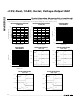
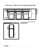
SCLK
DIN
COMMAND EXECUTED
98 16 (1)1
C2C3 D0C1 C0 D11 D10 D9 D6 D5 D4 D3 D2 D1D8 D7
CS
Figure 2. Serial-Interface Signals
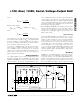
SCLK
DIN
DOUT
t
CS0
t
CSS
t
CP
t
CSH
t
CS1
t
CSW
t
CSD
t
LDS
t
LD
t
CH
t
DS
t
CSE
t
DO1
t
DH
t
CL
MSB
LSB
CS
LDAC
Figure 3. Serial-Interface Timing Diagram