
Datasheet


Detailed Description
The MAX5322 dual, 12-bit DAC operates from either
single or dual analog supplies. Dual ±12V to ±15V
power supplies provide bipolar ±5V to ±10V outputs, or
unipolar 0V to 10V outputs. Single 12V to 15V analog
power supplies only provide unipolar 0 to 10V outputs.
The reference inputs accept voltages from 2V to 5.25V.
The DAC features INL and DNL less than ±1 LSB (max),
a fast 10µs settling time, and a hardware shutdown
mode that reduces current consumption to 2.8µA. The
device features a 10MHz SPI-/QSPI-/MICROWIRE-com-
patible serial interface that operates with 3V or 5V logic,
an asynchronous load input, and a serial-data output.
The device offers a CLR that sets the DAC outputs to 0V.
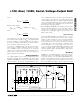
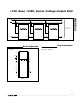
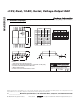
Figure 1 shows the functional diagram of the MAX5322.
Serial Interface
An SPI-/QSPI-/MICROWIRE-compatible serial interface
allows complete control of the DAC through a 16-bit
control word. The first 4 bits form the control bits that
determine register loading and software shutdown
functions. The last 12 bits form the DAC data. The 16-
bit word is entered MSB first.
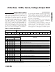
Table 1 shows the serial-data control-word format.
Table 2 shows the interface commands. The MAX5322
can be programmed while in shutdown.
The serial interface contains five registers: a 16-bit shift
register, two 12-bit input registers, and two 12-bit DAC
registers (Figure 1). The shift register accepts data
from the serial interface. The input registers act as
holding registers for data going to the DAC registers
MAX5322
±10V, Dual, 12-Bit, Serial, Voltage-Output DAC
______________________________________________________________________________________ 13
CONTROL BITS DATA BITS
MSB LSB
C3 C2 C1 C0 D11 D10 D9 D8 D7 D6 D5 D4 D3 D2 D1 D0
Table 1. Control-Word Format
16-BIT SERIAL WORD
CONTROL BITS DATA BITS
C3 C2 C1 C0 D11–D0
FUNCTION
0 0 0 0 XXXXXXXXXXXX No operation (NOP).
0 0 0 1 12-bit DAC data
Load both DAC registers and both input registers from the shift register.
(Start both DACs with new data.)
0 0 1 0 12-bit DAC data Load input register A from the shift register; DAC registers are unchanged.
0 0 1 1 12-bit DAC data Load input register B from the shift register; DAC registers are unchanged.
0 1 0 0 12-bit DAC data Load DAC register A and input register A from the shift register.
0 1 0 1 12-bit DAC data Load DAC register B and input register B from the shift register.
0 1 1 0 XXXXXXXXXXXX Update DAC register A from input register A (no data sent).
0 1 1 1 XXXXXXXXXXXX Update DAC register B from input register B (no data sent).
1 0 0 0 XXXXXXXXXXXX Shut down DAC A (provided SHDN = 1).
1 0 0 1 XXXXXXXXXXXX Shut down DAC B (provided SHDN = 1).
1 0 1 0 XXXXXXXXXXXX
Update both DAC registers from their respective input registers.
(Start both DACs with data previously stored in the input register.)
1 0 1 1 XXXXXXXXXXXX Shut down both DACs (provided SHDN = 1).
1 1 0 0 XXXXXXXXXXXX Power up DAC A (no change to any registers).
1 1 0 1 XXXXXXXXXXXX Power up DAC B (no change to any registers).
1 1 1 0 XXXXXXXXXXXX Power up both DACs (no change to any registers).
1 1 1 1 XXXXXXXXXXXX Not used.
Table 2. Serial-Interface Programming Commands
X = Don’t care.
Note: The DACs can be programmed in shutdown mode.