
Datasheet


MAX5322
±10V, Dual, 12-Bit, Serial, Voltage-Output DAC
12 ______________________________________________________________________________________
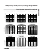
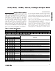
PIN NAME FUNCTION
1, 2, 13–16,
27, 28
N.C. No Connection. Not internally connected.
3 UNI/BIPB
DAC B Output-Mode Selection Input. Selects unipolar or bipolar output. Logic high = unipolar, logic
low = bipolar. In unipolar mode, the analog output range is 0 to 2 x V
REF
. In bipolar mode, the analog
output range is (-2 x V
REF
) to (+2 x V
REF
).
4 SHDN
Active-Low Shutdown Input. Pulling SHDN low forces the DAC buffers into high impedance. Drive
SHDN high for normal operation.
5 LDAC
Active-Low Load DAC Input. DAC A and DAC B are updated with information in the input register on
the LDAC falling edge.
6 CLR
Acti ve- Low Asynchr onous C l ear D AC Inp ut. P ul l i ng C LR l ow cl ear s al l D AC s and i np ut r eg i ster s; r esets
al l outp uts to zer o.
7 DGND Digital Ground
8V
CC
Digital Power Input. Connect V
CC
to a +2.7V to +5.5V power supply. Bypass V
CC
to DGND with a 10µF
and 0.1µF capacitor in parallel as close to the device as possible.
9DOUT
Serial-Data Output. Data is clocked out on SCLK’s falling edge. DOUT is high impedance when CS is
high. Data shifted into DIN appears at DOUT 16.5 clock cycles later.
10 SCLK Serial-Clock Input. SCLK clocks data in and out of the serial interface.
11 DIN Serial-Data Input. Data is clocked in on the rising edge of SCLK.
12 CS Active-Low Chip-Select Input. Data is not clocked into DIN unless CS is low.
17 UNI/BIPA
DAC A Output-Mode Selection. Selects unipolar or bipolar output. Logic high = unipolar, logic low =
bipolar. In unipolar mode, the analog output range is 0 to 2 x V
REF
. In bipolar mode, the analog output
range is (-2 x V
REF
) to (+2 x V
REF
).
18 OUTA DAC A Output
19 SGNDA DAC A Sense Ground. Connect to AGND.
20 REFA Reference Input for DAC A
21 V
DD
Positive Analog-Power Input. Connect V
DD
to a +10.8V to +15.75V power supply. Bypass V
DD
to
AGND with a 10µF and 0.1µF capacitor in parallel as close to the device as possible.
22 REFB DAC B Reference Input
23 AGND Analog Ground
24 SGNDB DAC B Sense Ground. Connect to AGND.
25 OUTB DAC B Output
26 V
SS
Negative Analog-Power Input. For single-supply operation, connect V
SS
to AGND. For dual-supply
operation, connect V
SS
to a -10.8V to -15.75V power supply and bypass V
SS
to AGND with a 10µF and
0.1µF capacitor in parallel, as close to the device as possible.
Pin Description