
Datasheet


39Maxim Integrated
MAX5318
18-Bit, High-Accuracy Voltage Output DAC with
Digital Gain, Offset Control, and SPI Interface
Offset Error
Offset error indicates how well the actual transfer func-
tion matches the ideal transfer function at a single point.
Typically, the point at which the offset error is specified
is at or near the zero-scale point of the transfer function.
Gain Error
Gain error is the difference between the ideal and the
actual full-scale output voltage on the transfer curve,
after nullifying the offset error. This error alters the slope
of the transfer function and corresponds to the same
percentage error in each step.
Settling Time
The settling time is the amount of time required from the
start of a LDAC high-to-low transition or BUSY low-to-high
transition (whichever occurs last), until the DAC output
settles to within 0.003% of the final value.
Digital Feedthrough
Digital feedthrough is the amount of noise that appears
on the DAC output when the DAC digital control lines are
toggled.
Digital-to-Analog Glitch Impulse
The glitch impulse occurs at the major carry transitions
along the segmented bit boundaries. It is specified as the
net area of the glitch impulse which appears at the output
when the digital input code changes by 1 LSB. The glitch
impulse is specified in nanovolts-seconds (nV-s).
Digital-to-Analog Power-Up Glitch Impulse
The digital-to-analog power-up glitch is the net area of
the glitch impulse which appears at the output when the
device exits power-down mode.
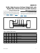
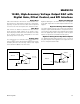
Figure 13. Unipolar High-Voltage Output
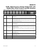
Figure 14. Bipolar Output
OUT
0V TO KV
REF
K = 1 + R2/R1
R2R1
MAX5318
MAX44250
OUT
REFO
-V
REF
TO
V
REF
R2
R1 = R2
R1
MAX5318
MAX9632