
Datasheet


37Maxim Integrated
MAX5318
18-Bit, High-Accuracy Voltage Output DAC with
Digital Gain, Offset Control, and SPI Interface
Power Supplies and
Bypassing Considerations
For best performance, use a separate supply for the
MAX5318. Bypass V
DDIO
, AVDD_, and AVSS with high-
quality ceramic capacitors to a low-impedance ground
as close as possible to the device. A typical high-quality
X5R 10FF capacitor can become self resonant at 2MHz.
Therefore, it is actually an inductor above 2MHz and is
useless for decoupling signals above 2MHz. It is there-
fore recommended that several capacitors of different
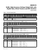
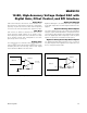
values are connected in parallel. Figure 10 shows the
magnitude of impedance of typical 1FF, 100nF, and
10nF X5R capacitors. As the capacitance reduces, the
self-resonant frequency increases. In addition, the paral-
lel combination of all three is shown and exhibits a sig-
nificant improvement over a single capacitor. These plots
do not include any PCB trace inductance.
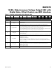
Minimize lead lengths to reduce lead inductance. Adding
just 2nH trace inductance to each of the typical capaci-
tors above produces the effects shown in Figure 11. This
shows significant reduction in the self-resonant frequen-
cies of the capacitors.
Internal Linear Regulator (BYPASS)
BYPASS is the output of an internal linear regulator and is
used to power digital circuitry. Connect BYPASS to DGND
with a ceramic capacitor in the range of 1FF to 10FF with
ESR in the range of 100mI to 20mI to ensure stability.
The typical voltage on this pin is 2.4V. Use a low-leakage
capacitor to ensure low power-down current.
Power-Supply Sequencing
During power-up, ensure that AVDD_ comes up before
the reference does. If this is not possible, connect a
Schottky diode between the REF and AVDD_ such as
the MBR0530T1G. If REF does come up before AVDD_,
the diode conducts and clamps REF to AVDD_. Once
AVDD_ has come up, the diode no longer conducts.
REF should always be below AVDD_ as specified in the
Electrical Characteristics. AVDD_ and AVDD_ should be
connected together and powered from the same supply.
V
DDIO
and AVSS can be sequenced in any order. Always
perform a reset operation after all the supplies are brought
up to place the device in a known operating state.
Layout Considerations
Digital and AC transient signals on AGND inputs can
create noise at the outputs. Connect both AGND inputs
to form the star ground for the DAC system. Refer remote
DAC loads to this system ground for the best possible
performance (see the Force/Sense section).
Use proper grounding techniques, such as a multilayer
board with a low-inductance ground plane, or star con-
nect all ground return paths back to AGND. Do not use
wire-wrapped boards and sockets. Use ground plane
shielding to improve noise immunity. Do not run analog
and digital signals parallel to one another (especially
clock signals) and avoid routing digital lines underneath
the device package.
For a recommended layout, consult the MAX5318
Evaluation Kit datasheet.
Figure 10. Typical X5R Capacitor Impedance
Figure 11. Typical X5R Capacitor Impedance with Additional
2nH PCB Trace Inductance
3k
1k
100
10
1
100m
10m
100k 1M 10M 100M
4m
IMPEDANCE (I)
FREQUENCY (Hz)
10nF
1µF
100nF
3k
1k
100
10
1
100m
10m
100k 1M 10M 100M
4m
IMPEDANCE (I)
FREQUENCY (Hz)
10nF
1µF
100nF
10nF
1µF
100nF