
Datasheet


34Maxim Integrated
MAX5318
18-Bit, High-Accuracy Voltage Output DAC with
Digital Gain, Offset Control, and SPI Interface
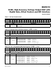
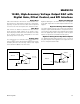
Table 15. General Configuration Write Register (0x4)
BIT 17 16 15 14 13 12 11 10 9 8 7 6 5 4 3 2 1 0
NAME
PD_SW NO_HOLDEN
RST_SW NO_BUSY
DOUT_ON X X X X X X X X X X X X X
DEFAULT
0 0 1 0 0 X X X X X X X X X X X X X
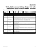
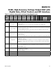
BIT NAME DESCRIPTION
17 PD_SW
Software PD (Power-Down). Equivalent to the PD input.
0: Normal mode
1: Power-down mode. OUT is internally connected to AGND using a 2kI resistor.
16 NO_HOLDEN
SPI Bus Hold Enable.
0: Bus hold enabled for SPI DOUT output. DOUT stays at its last value after the SPI CS
input rises at the end of the SPI frame (i.e. after the 24th clock cycle).
1: Bus hold disabled for SPI DOUT output. DOUT goes high impedance after the SPI CS
input rises at the end of the SPI frame (i.e. after the 24th clock cycle).
15
RST_SW
Software Reset. Equivalent to the RST input.
0: Place device in reset
1: Normal operation
Set the active low RST_SW bit low to initiate a software reset (equivalent to pulling RST low)
14
NO_BUSY
BUSY Input Disable.
0: BUSY input is active.
1: BUSY input is disabled.
Note that this does not affect the BUSY bit in the General Configuration and Status
Register. The BUSY pin is bidirectional. When enabled, it can be pulled down externally
to delay DAC updates.
13 DOUT_ON
SPI DOUT Output Disable. DOUT is disabled by default.
0: DOUT output disabled. When DOUT is disabled, the output is pulled low for the
duration of the SPI frame.
1: DOUT output enabled.
12:0 — Don’t care. These bits are reserved for the corresponding read command.