
Datasheet


33Maxim Integrated
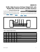
MAX5318
18-Bit, High-Accuracy Voltage Output DAC with
Digital Gain, Offset Control, and SPI Interface
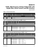
Table 13. OFFSET Register Write in Two’s Complement (0x2)
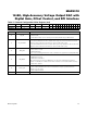
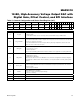
Table 14. GAIN Write Register (0x3)
BIT 17 16 15 14 13 12 11 10 9 8 7 6 5 4 3 2 1 0
NAME
B17 B16 B15 B14 B13 B12 B11 B10 B9 B8 B7 B6 B5 B4 B3 B2 B1 B0
DEFAULT
0x00000—Zero Offset
BIT NAME DESCRIPTION
17:0 B[17:0]
18-bit offset code in two’s complement format. For clarity, a few examples are shown below:
10 0000 0000 0000 0000 0x20000 offset of -2
17
11 1111 1111 1111 1111 0x3FFFF offset of -1
00 0000 0000 0000 0000 0x00000 offset of 0
00 0000 0000 0000 0001 0x00001 offset of +1
01 1111 1111 1111 1111 0x1FFFF offset of 2
17
– 1
BIT 17 16 15 14 13 12 11 10 9 8 7 6 5 4 3 2 1 0
NAME
B17 B16 B15 B14 B13 B12 B11 B10 B9 B8 B7 B6 B5 B4 B3 B2 B1 B0
DEFAULT
0x3FFFF—Gain of 1
BIT NAME DESCRIPTION
17:0 B[17:0]
18-bit gain code. For clarity, a few examples are shown below:
11 1111 1111 1111 1111 3FFFF\h Gain of 1. (2
18
– 1 + 1)/2
18
11 1111 1111 1111 1110 3FFFE\h Gain of 0.999996. (2
18
– 2 + 1)/2
18
01 1111 1111 1111 1111 1FFFF\h Gain of 0.5. (2
17
– 1 + 1)/2
18
01 1111 1111 1111 1110 1FFFE\h Gain of 0.499996. (2
17
– 2 + 1)/2
18
00 0000 0000 0000 0000 00000\h Gain of 0.0000076. 1/2
18