
Datasheet


31Maxim Integrated
MAX5318
18-Bit, High-Accuracy Voltage Output DAC with
Digital Gain, Offset Control, and SPI Interface
Command and Register Map
All command and data registers have read and write
functionality. The register selected depends on the com-
mand select bits R[3:0]. Each write to the device consists
of 4 command select bits (R[3:0]), 18 data bits (which are
detailed in Table 11 to Table 19), and 2 don’t care LSBs.
A summary of the commands is shown in Table 10.
Applications Information
Power-On Reset (POR)
Upon power-on, the output is set to either zero-scale
(if M/Z is low) and midscale (if M/Z is high). The entire
register map is set to their default values as shown in
Table 11 to Table 19.
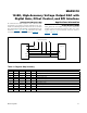
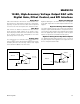
Figure 9. Stand-Alone Operation
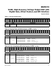
Table 10. Register Map Summary
CSm
CS1
CS
CS
SCLK
µC
DWRITE
DREAD
SCLK
DIN
DOUT
MAX5318
TO OTHER DEVICES/CHAINS
HEX R3 R2 R1 R0 FUNCTION
0 0 0 0 0 No-op. Used mainly in daisy-chain communications.
1 0 0 0 1 DIN register write
2 0 0 1 0 OFFSET register write
3 0 0 1 1 GAIN register write
4 0 1 0 0 Configuration register write
5–8 — — — — Reserved
9 1 0 0 1 DIN register read
A 1 0 1 0 OFFSET register read
B 1 0 1 1 GAIN register read
C 1 1 0 0 Configuration and status register read.
D–F — — — — Reserved