
Datasheet


3Maxim Integrated
MAX5318
18-Bit, High-Accuracy Voltage Output DAC with
Digital Gain, Offset Control, and SPI Interface
ELECTRICAL CHARACTERISTICS (continued)
(V
AVDD
= V
DDIO
= 4.5V to 5.5V, V
AVSS
= -1.25V, V
AGND
= V
DGND
= V
AGND_F
= V
AGND_S
= 0V, V
REF
= 4.096V, TC/SB =
PD = LDAC = M/Z = DGND, RST = V
DDIO
, C
REFO
= 100pF, C
L
= 100pF, R
L
= 10kω, C
BYPASS
= 1µF, T
A
= -40°C to +105°C, unless
otherwise noted. Typical values are at T
A
= +25°C.) (GAIN = 0x3FFFF and OFFSET = 0x00000.)(Note 2)
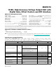
PARAMETER SYMBOL CONDITIONS MIN TYP MAX UNITS
Reset Voltage Output V
OUT-RESET
RST = pulse low
M/Z = DGND
75
FV
M/Z = V
DDIO
2.048 V
RST = pulse low,
V
AVSS
= 0V
M/Z = DGND
10 mV
M/Z = V
DDIO
2.048 V
RST = DGND
M/Z = DGND
-68 mV
M/Z = V
DDIO
2.036 V
RST = DGND,
V
AVSS
= 0V
M/Z = DGND
10 mV
M/Z = V
DDIO
2.036 V
DC Output Impedance (Normal
Mode)
R
OUT
Closed-loop connection (RFB connected
to OUT)
4
mI
Output Resistance (Power-Down
Mode)
PD = V
DDIO
2
kI
Output Current I
OUT
Source/sink within 100mV of the supply
rails
Q4
mA
Source/sink within 800mV of the supply
rails
Q25
Load Capacitance to GND C
L
200 pF
Load Resistance to GND R
L
For specified performance 2
kI
Short-Circuit Current I
SC
OUT shorted to AGND or AVDD
Q60
mAREFO shorted to AGND or AVDD
Q65
BYPASS shorted to AGND or AVDD
Q48
Short-Circuit Duration T
SC
Short to AGND or AVDD
Indefinite
s
DC Power-Supply Rejection DC PSRR
V
OUT
at full scale, V
AVDD
= 4.5V to 5.5V -2.5
Q0.20
+2.5
LSB/V
V
AVSS
= -1.5V to -0.5V -2.5
Q0.012
+2.5
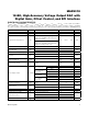
STATIC PERFORMANCE—VOLTAGE REFERENCE INPUT SECTION
Reference High Input Range V
REF
2.4
V
AVDD
-
0.1
V
Reference Input Capacitance C
REF
10 pF
Reference Input Resistance R
REF
10
MI
Reference Input Current I
B
Q0.15 FA
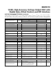
STATIC PERFORMANCE—VOLTAGE REFERENCE OUTPUT SECTION
Reference High Output Range 2.4
V
AVDD
-
0.1
V
Reference High Output Load
Regulation
500
ppm/
mA
Reference Output Capacitor
R
ESR
< 5I
0.1 nF