
Datasheet


27Maxim Integrated
MAX5318
18-Bit, High-Accuracy Voltage Output DAC with
Digital Gain, Offset Control, and SPI Interface
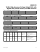
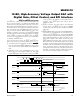
Numerical Examples
Several numerical examples for the MAX5318, as shown
in Table 7 and Table 8, illustrate how the gain and off-
set control changes the output voltage. The examples
assume a reference voltage of 4.096V. Note that if the
result of the calculation results in an under- or over-range
output voltage, V
OUT
is set to its zero or full-scale value,
respectively. An under-range output is less than 0V and
an over-range output is greater than V
REF
- 1 LSB.
Reset
The device is reset upon power-on, hardware reset using
RST, or software reset using register 0x4, bit 15, com-
mand RSTSW. After reset, the value of the input register,
the DAC latch and the output voltage are set to the values
defined by the M/Z input. If a hardware reset occurs dur-
ing a SPI programming frame, anything before and after
the reset for the frame will be ignored. A software reset
initiated through the SPI interface takes effect after the
end of the valid frame.
Output State Upon Reset
The output voltage can be set to either zero or mid-
scale upon power-up, or a hardware or software reset,
depending on the state of the M/Z input. After power-up,
if the device detects that this input is low, the output volt-
age is set to zero scale. If M/Z is high, the output voltage
is set to midscale.
Note that during reset, when RST is low or RSTSW is set
to 0, the output voltage is set slightly lower than the value
after coming out of reset. During reset, the output voltage
is set to the values shown for the V
OUT-RESET
specifica-
tion in the Electrical Characteristics.
Power-Down
The device can be powered down by either hardware
(pulling PD high) or software (setting the PD_SW bit in
either the 0x4 or 0xC registers). Note that the hardware
and software inputs are ORed. Asserting either is enough
to place the device in power-down mode.
In order to restore normal operation to the device, satisfy
both of these conditions:
1) Pull PD low.
2) Set the bits PD_SW’s (in both 0x4 and 0xC registers)
to 0.
In power-down, the output is internally connected to
AGND through a 2kI resistor. The SPI interface remains
active and the DAC register content remains unchanged.
Data Format Selection
(Straight Binary vs. Two’s Complement)
The MAX5318 interprets the data code input (DIN) as
either straight binary or two’s complement. To choose the
straight binary format, set the TC/SB input low. For two’s
complement, set the input high.
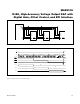
Table 8. Two’s Complement DIN Examples
DIN V
DIN
(V) GAIN G OFFSET V
OFFSET
(V) CALCULATION COMMENT
0x30000 -1.024 0x2FFFF 0.75 0x08000 0.512
V
OUT
= 4.096/2
+ 0.75 x (-1.024)
+ 0.512 = 1.792V
• For V
OUT
, use Equation 4
• For V
DIN
, use Table 1b first formula
• For G, use Table 2
• For V
OFFSET
, use Table 3 second
formula
0x10000 1.024 0x0FFFF 0.25 0x38000 -0.512
V
OUT
= 4.096/2
+ 0.25 x 1.024
- 0.512 = 1.792V
• For V
OUT
, use Equation 4
• For V
DIN
, use Table 1b first formula
• For G, use Table 2
• For V
OFFSET
, use Table 3 first
formula