
Datasheet


26Maxim Integrated
MAX5318
18-Bit, High-Accuracy Voltage Output DAC with
Digital Gain, Offset Control, and SPI Interface
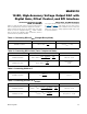
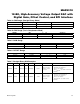
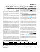
Table 6. OFFSET Range
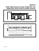
Table 7. Straight Binary DIN Examples
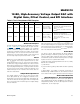
Table 4a. DIN Range (Straight Binary Mode)
Table 4b. DIN Range (Two’s Complement Mode)
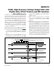
Table 5. GAIN Range
RANGE OFFSET V
OFFSET
(V) VALUE (V)
Minimum 0x20000 -V
REF
/2 -2.048
Maximum 0x1FFFF (V
REF
/2 - 1 LSB) 2.047992188
DIN V
DIN
(V) GAIN G OFFSET V
OFFSET
(V) CALCULATION COMMENT
0x20000 2.048 0x2FFFF 0.75 0x10000 1.024
V
OUT
= 0.75 x
2.048 + 1.024
= 2.56V
• For V
OUT
, use Equation 3
• For V
DIN
, use Table 1a
• For G, use Table 2
• For V
OFFSET
, use Table 3 second
formula
0x30000 3.072 0x0FFFF 0.25 0x30000 -1.024
V
OUT
= 0.25 x
3.072 - 1.024
= 0.512V
• For V
OUT
, use Equation 3
• For V
DIN
, use Table 1a
• For G, use Table 2
• For V
OFFSET
, use Table 3 first
formula
RANGE DIN V
DIN
(V) VALUE (V)
Minimum 0x00000 0 0
Maximum 0x3FFFF (V
REF
- 1 LSB) 4.095984375
RANGE DIN V
DIN
(V) VALUE (V)
Minimum 0x20000 0 0
Maximum 0x1FFFF (V
REF
- 1 LSB) 4.095984375
RANGE GAIN G VALUE (V)
Minimum 0x00000 1/2
18
0.0000038147
Maximum 0x3FFFF 1 1