
Datasheet


25Maxim Integrated
MAX5318
18-Bit, High-Accuracy Voltage Output DAC with
Digital Gain, Offset Control, and SPI Interface
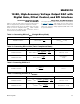
Conversion Formulas for DIN,
GAIN, and OFFSET
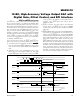
Tables 1a and 1b show how to convert the DIN code to
V
DIN
in straight binary and two’s complement modes.
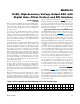
Table 2 shows how to convert the GAIN code to the gain
factor G, which is multiplied with V
DIN
. Table 3 shows
how to convert the OFFSET code to V
OFFSET
, which is
summed with the product G•V
DIN
.
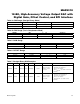
Input, Gain, and Offset Ranges
The ranges of DIN, GAIN, and OFFSET are summarized
in Table 4 to Table 6. Also shown are the range values
for the 18-bit MAX5318 with a 4.096V reference. Note that
V
REF
is the reference voltage applied to REF and 1 LSB
is equal to V
REF
/2
18
.
Table 1a. Converting DIN to V
DIN
(Straight Binary Mode)
Table 2. Converting GAIN to G
Table 3. Converting OFFSET to V
OFFSET
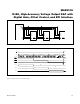
Table 1b. Converting DIN to V
DIN
(Two’s Complement Mode)
DIN EQUATION FOR V
DIN
RANGE
0x00000 to 0x3FFFF
DIN REF
18
DIN
VV
2
= ×
0V to (V
REF
- 1 LSB)
OFFSET EQUATION RANGE
0x20000 to 0x3FFFF -V
REF/2 to -1 LSB
0x00000 to 0x1FFFF 0V to (V
REF/2 - 1 LSB)
DIN EQUATION FOR V
DIN
AND V
OFFSET
RANGE
0x20000 to 0x3FFFF V
REF
/2 to -1 LSB
0x00000 to 0x1FFFF
0V to (V
REF
/2 -
1 LSB)
REF
DIN REF
18
V
DIN - 0x20000
VV -
2
2
= ×
DIN REF
18
CODE
VV
2
= ×
GAIN EQUATION RANGE
0x00000 to 0x3FFFF 1/2
18
to 1
18
GAIN 1
G
2
+
=
REF
OFFSET REF
18
V
OFFSET 0x20000
VV
2
2
−
=×−
OFFSET REF
18
OFFSET
VV
2
= ×