
Datasheet


24Maxim Integrated
MAX5318
18-Bit, High-Accuracy Voltage Output DAC with
Digital Gain, Offset Control, and SPI Interface
The data DIN can be either straight binary or two’s com-
plement. In straight binary, zero code results in a zero-
scale output. In two’s complement, zero code results in
a midscale output.
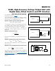
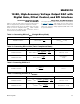
To better understand how GAIN and OFFSET affect the
output voltage, see Figure 4 and Figure 5. Consider
the generation of a ramp. For now assume OFFSET
is set to 0x00000. In straight binary mode, with GAIN
set to 0x3FFFF (G = 1), DIN starts from 0x00000 and
increases to 0x3FFFF. The output voltage will start at 0V
and increase to (V
REF
- 1 LSB). If GAIN is reduced, the
ramp will still start at 0V but the maximum level reached
is reduced.
With DIN set to two’s complement mode, to generate the
same ramp, DIN would start at 0x20000 and increase
until it wraps around to 0x00000. At this point the
DAC output would be midscale. DIN then increases to
0x1FFFF where the output would be full-scale -1 LSB. As
GAIN is reduced, the start of the ramp becomes larger
and the end of the ramp becomes smaller. The ramp is
therefore centered at midscale.
In both cases, a nonzero value for OFFSET results in the
output moving up or down.
Should the output of the gain and offset adjust block
overflow full-scale or underflow zero-scale, the data is
clipped so the DAC output will be clipped rather than
overflow or underflow.
The effect of gain and offset adjustment is shown in
Figure 4 for straight binary mode and Figure 5 for two’s
complement mode.
If any of the DIN, GAIN, or OFFSET registers is changed,
the device takes 1.9µs (t
BUSY
) to compute the new val-
ues to present to the DAC. While the device is computing
the new DAC value, the BUSY output is set low. See the
section on the BUSY output and LDAC input for details.
Figure 4. Gain and Offset Adjustment in Straight Binary Mode
Figure 5. Gain and Offset Adjustment in Two’s Complement
Mode
POSITIVE OFFSET
FULL-SCALE
V
OUT
V
REF
0V
00000h20000h
MIDSCALE
GAIN < 0x3FFFF (G < 1)
ZERO-SCALE
DIN
IDEAL CHARACTERISTIC
NEGATIVE OFFSET
3FFFFh
POSITIVE OFFSET
FULL-SCALE
V
OUT
V
REF
0V
20000h00000h
MIDSCALE
GAIN < 0x3FFFF (G < 1)
ZERO-SCALE
DIN
IDEAL CHARACTERISTIC
NEGATIVE OFFSET
1FFFFh