
Datasheet


23Maxim Integrated
MAX5318
18-Bit, High-Accuracy Voltage Output DAC with
Digital Gain, Offset Control, and SPI Interface
18-Bit Ideal Transfer Function
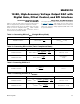
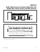
The MAX5318 features 18-bit gain and 18-bit offset
adjustment as shown in Figure 3.
The incoming DIN code is multiplied and offset compen-
sated by the generic equation shown in Equation 1. The
resulting value is then applied to the DAC.
Equation 1) Generic gain and offset adjustment
DAC DIN GAIN OFFSET=×+
The GAIN code is always an 18-bit straight binary word.
The OFFSET code is always two’s complement. It is
therefore simply added to the output of the multiplier.
To
guarantee that a gain of exactly 1 is possible, the
actual gain coefficient applied to DIN is as defined in
Equation 2.
Equation 2) Calculation of gain
( )
18
GAIN 1
G
2
+
=
When DIN is straight binary, the ideal transfer function is
given by:
Equation 3) Straight binary ideal transfer function
OUT DIN OFFSET
V GV V=×+
When DIN is two’s complement, the ideal transfer func-
tion is given by:
Equation 4) Two’s complement ideal transfer function
REF
OUT DIN OFFSET
V
V GV V
2
= +× +
V
DIN
and V
OFFSET
are the voltages to which the DIN and
OFFSET codes are converted and V
OUT
is the voltage at
the DAC output buffer. See the Conversion Formulas for
DIN, GAIN, and OFFSET section for equations needed
to convert the DIN and OFFSET codes into V
DIN
and
V
OFFSET
.
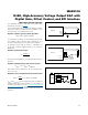
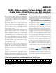
Figure 2a. Star Ground Connection
Figure 2b. Force/Sense Connection
Figure 3. Gain and Offset Adjustment
OUT
RFB
AGND_F
AGND_S
AGND
MAX5318
OUT
RFB
AGND
AGND_F
AGND_S
MAX5318
SPI
INTERFACE
OFFSET
GAIN
DIN
DAC
REGISTER
LDAC