
Datasheet


21Maxim Integrated
MAX5318
18-Bit, High-Accuracy Voltage Output DAC with
Digital Gain, Offset Control, and SPI Interface
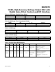
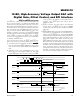
Pin Description (continued)
PIN NAME FUNCTION
5 LDAC
Active-Low Load DAC Logic Input. If LDAC is taken low while BUSY is inactive (high), the contents of the
input registers are transferred to the DAC register and the DAC output is updated. If LDAC is taken low
while BUSY is asserted low, the LDAC event is stored and the DAC register update is delayed until BUSY
deasserts. Any event on LDAC during power-on reset or when RST is low is ignored.
6 DOUT SPI Bus Serial Data Output. See the Serial Interface section for details.
7 DIN SPI Bus Serial Data Input. See the Serial Interface section for details.
8 SCLK SPI Bus Serial Clock Input. See the Serial Interface section for details.
9 CS SPI Bus Active-Low Chip-Select Input. See the Serial Interface section for details.
10 TC/SB
DIN Format Select Input. Connect TC/SB to DGND to set the data input format to straight binary or to
V
DDIO
to set it to two’s complement.
11 PD
Active-High Power-Down Input. Connect PD to DGND for normal operation. Connect PD to V
DDIO
to
place the device in power-down. In power-down, OUT (analog voltage output) is connected to AGND
through a 2kω resistor, but the contents of the input registers and the DAC latch do not change. The SPI
interface remains active in power-down.
12 AVSS
Negative Analog Power-Supply Input. Connect to AGND or a negative supply voltage. When connected
to the negative supply voltage, bypass AVSS with a 0.1µF capacitor to AGND.
13 AGND Analog Ground. Connect to the analog ground plane.
14 AVDD1
Positive Analog Power-Supply Input. Bypass each AVDD_ locally with a 0.1µF and 10µF capacitor to
AGND (analog ground plane). Connect AVDD1 and AVDD2 together.
15 OUT
Buffered Analog Voltage Output. Connect OUT to RFB externally to close the output buffer feedback
loop. The buffered output is capable of directly driving a 10kω load. The state of M/Z sets the power-
on reset state of OUT (zero or midscale). In power-down, OUT is connected to AGND through a 2kω
pulldown resistor.
16 RFB
Feedback Resistor Input. RFB is connected through the internal feedback resistor to the inverting input of
the analog output buffer. Externally connect RFB to OUT to close the output buffer feedback loop.
17 REFO Voltage Reference Buffered Output. Bypass with a 100pF capacitor to AGND.
18 REF High-Impedance 10Mω Voltage Reference Input
19 AGND_S DAC Analog Ground Sense
20 AGND_F DAC Analog Ground Force. Connect to the analog ground plane.
21 AVDD2
Positive Analog Power-Supply Input. AVDD2 supplies power to the internal digital linear regulator. Bypass
AVDD2 locally to AGND with 0.1µF and 10µF capacitors. Connect AVDD2 and AVDD1 together.
22 BYPASS Internal Bypass Connection. Connect BYPASS to DGND with 0.01µF and 1µF capacitors.
23 DGND Digital Ground
24 V
DDIO
Digital Interface Power-Supply Input. Connect to a 1.8V to 5.5V logic-level supply. Bypass V
DDIO
with a
0.1µF capacitor to DGND. The supply voltage at V
DDIO
sets the logic-level for the digital interface.