
Datasheet

20Maxim Integrated
MAX5318
18-Bit, High-Accuracy Voltage Output DAC with
Digital Gain, Offset Control, and SPI Interface
Pin Description
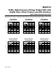
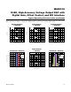
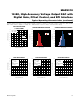
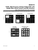
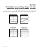
Pin Configuration
M/Z
DOUT
DIN
SCLK
CS
AVDD2
AGND_F
AGND_S
REF
REFO
RST
V
DDIO
DGND
BYPASS
RFB
OUT
TC/SB
PD
AVSS
AGND
AVDD1
BUSY
LDAC
READY
24
23
22
21
20
19
18
1
2
3
4
5
6
7
TOP VIEW
MAX5318
178
169
1510
1411
1312
TSSOP
+
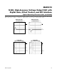
PIN NAME FUNCTION
1 RST
Active-Low Reset Input. Drive RST low to DGND to put the device into a reset state. A reset state sets all
SPI input registers to their default power-on reset states as defined by the state of inputs M/Z and TC/SB.
Set RST high to VDDIO, the DAC output remains at the state defined by M/Z until LDAC is taken low.
2 READY
SPI Active-Low Ready Output. READY asserts low when the device successfully completes processing
an SPI data frame. READY asserts high at the next rising edge of CS. In daisy-chain applications, the
READY output typically drives the CS input of the next device in the chain or a GPIO of a microcontroller.
3 M/Z
Reset Select Input. M/Z selects the default state of the analog output (OUT) after power-on or a hardware
or software reset. Connect M/Z to V
DDIO
to set the default output voltage to midscale or to DGND to set
the default output voltage to zero scale.
4 BUSY
Digital Input/Open-Drain Output. Connect a 2kI pullup resistor from BUSY to V
DDIO
. BUSY goes low
during the internal calculations of the DAC register data. During this time, the user can continue writing
new data to the DIN, OFFSET, and GAIN registers, but no further updates to the DAC register and
DAC output can take place. If LDAC is asserted low while BUSY is low, this event is stored. BUSY is
bidirectional, and can be asserted low externally to delay LDAC action. BUSY also goes low during
power-on reset, when RST is low, or when software reset is activated.