
Datasheet


4 Maxim Integrated
14-/16-Bit, Low-Power, Buffered Output,
Rail-to-Rail DACs with SPI Interface
MAX5214/MAX5216
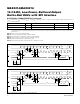
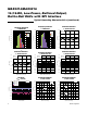
Figure 1. 16-Bit Serial-Interface Timing Diagram (MAX5214)
Figure 2. 24-Bit Serial-Interface Timing Diagram (MAX5216)
ELECTRICAL CHARACTERISTICS (continued)
(V
DD
= 2.7V to 5.5V, V
REF
= 2.5V to V
DD
, C
L
= 60pF, R
L
= 10kI, T
A
= -40NC to +105NC, unless otherwise noted. Typical values are
at T
A
= +25NC.) (Note 2)
Note 2: Electrical specifications are production tested at T
A
= +25NC and T
A
= +105NC. Specifications over the entire operating
temperature range are guaranteed by design and characterization. Typical specifications are at T
A
= +25NC and are not
guaranteed.
Note 3: Static accuracy tested without load.
Note 4: Linearity is tested within 20mV of GND and V
DD
.
Note 5: Gain and offset is tested within 100mV of GND and V
DD
.
Note 6: Subject to offset and gain error limits and V
REF
settings.
Note 7: Guaranteed by design; not production tested.
Note 8: All timing specifications measured with V
IL
= V
GND
, V
IH
= V
DD
.
DIN15
123 45 1678
14 15 16
DIN14 DIN13
t
DS
t
DH
t
CP
DIN12 DIN11 DIN10 DIN9 DIN8 DIN2 DIN1 DIN0 DIN15DIN
SCLK
CS
t
CSH0
t
CH
t
CL
t
CSS0
t
CSA
t
CLPW
t
CSC
t
CSF
t
CSPW
CLR
t
CSH1
DIN23 DIN22 DIN21 DIN20 DIN19 DIN18 DIN17 DIN16 DIN2 DIN1 DIN0 DIN23
123 45678
22 23 24 1
DIN
SCLK
CS
t
CSH1
t
CSA
t
CSF
t
CLPW
t
CSC
t
CSPW
CLR
t
DS
t
DH
t
CP
t
CH
t
CL
t
CSH0
t
CSS0
PARAMETER SYMBOL CONDITIONS MIN TYP MAX UNITS
CLR Pulse-Width Low t
CLPW 20 ns
CLR Rise to CS Fall t
CSC 20 ns