
Datasheet


MAX5186/MAX5189
Dual, 8-Bit, 40MHz, Current/Voltage,
Simultaneous-Output DACs
_______________________________________________________________________________________ 9
Applications Information
Static and Dynamic
Performance Definitions
Integral Nonlinearity (INL)
Integral nonlinearity is the deviation of the values on an
actual transfer function from either a best straight-line fit
(closest approximation to the actual transfer curve) or a
line drawn between the endpoints of the transfer func-
tion, once offset and gain errors have been nullified.
The MAX5186/MAX5189 use a straight-line endpoint fit
for INL (and DNL) and the deviations are measured at
every individual step.
Differential Nonlinearity (DNL)
Differential nonlinearity is the difference between an
actual step height and the ideal value of 1LSB. A DNL
error specification no more negative than -1LSB guar-
antees a monotonic transfer function.
Offset Error
The offset error is the difference between the ideal and
the actual offset current/voltage. For the MAX5186/
MAX5189, the offset error is the midpoint value of the
transfer function determined by the endpoints of a
straight-line endpoint fit. This error affects all codes by
the same amount.
Gain Error
Gain error is the difference between the ideal and the
actual output value range. This range represents the
output when all digital inputs are set to 1 minus the out-
put when all digital inputs are set to 0.
Glitch Impulse
A glitch is generated when a DAC switches between
two codes. The largest glitch is usually generated
around the midscale transition, when the input pattern
transitions from 011…111 to 100…000. This occurs due
to timing variations between the bits. The glitch impulse
is found by integrating the voltage of the glitch at the
midscale transition over time. The glitch impulse is usu-
ally specified in pV-s.
Settling Time
The settling time is the amount of time required from the
start of a transition until the DAC output settles its new
output value to within the converter’s specified accuracy.
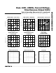
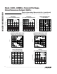
9.6kΩ*
REFR
REFO
1.2V REF
REN
CURRENT-
SOURCE ARRAY
DAC1 SWITCHES
DAC2 SWITCHES
400Ω*
OUT1P
OUT1N
OUT2N
OUT2N
400Ω* 400Ω* 400Ω*
MSB
DECODE
CLK
OUTPUT
LATCHES
OUTPUT
LATCHES
INPUT
LATCHES
*INTERNAL 400Ω AND 9.6kΩ
RESISTORS FOR MAX5189 ONLY.
INPUT
LATCHES
AV
DD
AGND CS DACEN PD
DV
DD
DGND
CREF1
CREF2
MAX5186
MAX5189
MSB
DECODE
D7–D0
Figure 1. Functional Diagram