
Datasheet


MAX5182/MAX5185
Dual, 10-Bit, 40MHz Current/Voltage
Alternate-Phase Output DACs
12 ______________________________________________________________________________________
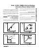
Gain Error
Gain error (Figure 5d) is the difference between the
ideal and the actual full-scale output voltage on the
transfer curve, after nullifying the offset error. This error
alters the slope of the transfer function and corre-
sponds to the same percentage error in each step.
Settling Time
Settling time is the amount of time required from the start
of a transition until the DAC output settles its new output
value to within the converter’s specified accuracy.
Digital Feedthrough
Digital feedthrough is the noise generated on a DAC’s
output when any digital input transitions. Proper board
layout and grounding will significantly reduce this
noise, but there will always be some feedthrough
caused by the DAC itself.
Total Harmonic Distortion
Total harmonic distortion (THD) is the ratio of the RMS
sum of the input signal’s first four harmonics to the fun-
damental itself. This is expressed as:
where V
1
is the fundamental amplitude, and V
2
through
V
5
are the amplitudes of the 2nd- through 5th-order
harmonics.
Spurious-Free Dynamic Range
Spurious-free dynamic range (SFDR) is the ratio of RMS
amplitude of the fundamental (maximum signal compo-
nent) to the RMS value of the next-largest distortion
component.
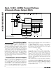
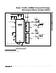
Differential to Single-Ended Conversion
The MAX4108 low-distortion, high-input bandwidth
amplifier may be used to generate a voltage from the
MAX5182’s current array output. The differential voltage
across OUT1P (or OUT2P) and OUT1N (or OUT2N) is
converted into a single-ended voltage by designing an
appropriate operational amplifier configuration as
shown in Figure 6.
Grounding and Power-Supply Decoupling
Grounding and power-supply decoupling strongly influ-
ence the performance of the MAX5182/MAX5185.
Unwanted digital crosstalk may couple through the
input, reference, power-supply, and ground connec-
tions, which may affect dynamic specifications like sig-
nal-to-noise ratio or SFDR. In addition, electromagnetic
interference (EMI) can either couple into or be generat-
ed by the MAX5182/MAX5185. Therefore, grounding
and power-supply decoupling guidelines for high-
speed, high-frequency applications should be closely
followed.
First, a multilayer PC board with separate ground and
power-supply planes is recommended. High-speed
signals should run on controlled impedance lines
directly above the ground plane. Since the MAX5182/
MAX5185 have separate analog and digital ground
buses (AGND and DGND, respectively), the PC board
should also have separate analog and digital ground
sections with only one point connecting the two. Digital
signals should run above the digital ground, and plane
and analog signals should run above the analog
ground plane.
Both devices have two power-supply inputs: analog
V
DD
(AV
DD
) and digital V
DD
(DV
DD
). Each AV
DD
input
should be decoupled with parallel 10µF and 0.1µF
ceramic chip capacitors as close to the pin as possi-
ble. Their opposite ends should have the shortest pos-
sible connection to the ground plane. The DV
DD
pins
should also have separate 10µF and 0.1µF capacitors,
again adjacent to their respective pins. Try to minimize
the analog load capacitance for proper operation. For
best performance, it is recommended to bypass CREF1
and CREF2 with low-ESR 0.1µF capacitors to AV
DD
.
The power-supply voltages should also be decoupled
at the point they enter the PC board with large tantalum
or electrolytic capacitors. Ferrite beads with additional
decoupling capacitors forming a pi network could also
improve performance.
THD
VVVV
V
=×
+++
20
2
2
3
2
4
2
5
2
1
log