
Datasheet


MAX5182/MAX5185
Dual, 10-Bit, 40MHz Current/Voltage
Alternate-Phase Output DACs
10 ______________________________________________________________________________________
PD
(POWER-DOWN SELECT)
DACEN
(DAC ENABLE)
POWER-DOWN MODE OUTPUT STATE
0 0 Standby
MAX5182 High-Z
MAX5185 AGND
0 1 Wake-Up Last state prior to standby mode
1 X Shutdown
MAX5182 High-Z
MAX5185 AGND
Table 1. Power-Down Mode Selection
X = Don’t care
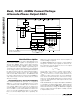
External Reference
To disable the MAX5182/MAX5185’s internal reference,
connect REN to DV
DD
. A temperature-stable, external
reference may now be applied to drive the REFO pin
(Figure 3) to set the full-scale output. Be sure to choose
a reference capable of supplying at least 150µA to
drive the bias circuit that generates the cascode cur-
rent for the current array. For improved accuracy and
drift performance, chose a fixed output voltage refer-
ence such as the +1.2V, 25ppm/°C MAX6520 bandgap
reference.
Standby Mode
To enter the lower power standby mode, connect digital
inputs PD and DACEN to DGND. In standby, both the
reference and the control amplifier are active, with the
current array inactive. To exit this condition, DACEN
must be pulled high with PD held at DGND. The
MAX5182/MAX5185 typically require 50µs to wake up
and let both outputs and reference settle.
Shutdown Mode
For lowest power consumption, the MAX5182/MAX5185
provide a power-down mode in which the reference,
control amplifier, and current array are inactive and the
DACs supply current is reduced to 1µA. To enter this
mode, connect PD to DV
DD
. To return to active mode,
connect PD to DGND and DACEN to DV
DD
. About 50µs
are required for the devices to leave the shutdown
mode and to settle their outputs to the values prior to
shutdown. Table 1 lists the power-down mode selection.
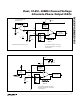
Timing Information
Both internal DAC cells write to their outputs in alternate
phase (Figure 4). The input latch of the first DAC
(DAC1) is loaded after the clock signal transitions high.
When the clock signal transitions low, the input latch of
the second DAC (DAC2) is loaded. The contents of the
first input latch are shifted into the DAC1 register on the
rising edge of the clock; the contents of the second
input latch are shifted into the input register of DAC2 on
the falling edge of the clock. Both outputs are updated
on alternate phases of the clock.
CLK
D0–D9
OUT1 N - 2
DAC1 DAC2 DAC1 DAC2 DAC1 DAC2
N - 1
N - 1
N - 1
N
N
N
N + 1 N + 1
t
DS1
t
CH
t
CL
t
CLK
OUT2
N - 1
N - 2
N
t
DS1
t
DH1
t
DH2
Figure 4. Timing Diagram