
Datasheet


MAX5180/MAX5183
Dual, 10-Bit, 40MHz, Current/Voltage
Simultaneous-Output DACs
______________________________________________________________________________________ 13
grounding and power-supply decoupling guidelines for
high-speed, high-frequency applications should be
closely followed.
First, a multilayer pc board with separate ground and
power-supply planes is recommended. High-speed
signals should be run on controlled impedance lines
directly above the ground plane. Since the MAX5180/
MAX5183 have separate analog and digital ground
buses (AGND and DGND, respectively), the PC board
should also have separate analog and digital ground
sections with only one point connecting the two. Digital
signals should run above the digital ground plane, and
analog signals should run above the analog ground
plane.
Both devices have two power-supply inputs: analog
V
DD
(AV
DD
) and digital V
DD
(DV
DD
). Each AV
DD
input
should be decoupled with parallel 10µF and 0.1µF
ceramic-chip capacitors. These capacitors should be as
close to the pin as possible, and their opposite ends
should be as close to the ground plane as possible. The
DV
DD
pins should also have separate 10µF and 0.1µF
capacitors adjacent to their respective pins. Try to mini-
mize analog load capacitance for proper operation. For
best performance, it is recommended to bypass CREF1
and CREF2 with low-ESR 0.1µF capacitors to AV
DD
.
The power-supply voltages should also be decoupled
with large tantalum or electrolytic capacitors at the
point they enter the PC board. Ferrite beads with addi-
tional decoupling capacitors forming a pi network can
also improve performance.
Chip Information
TRANSISTOR COUNT: 9464
SUBSTRATE CONNECTED TO AGND
BP
FILTER
CARRIER
FREQUENCY
MAX2452
IF
Q COMPONENT
BP
FILTER
3V
QUADRATURE
MODULATOR
I COMPONENT
0°
90°
Σ
3V
MAX5180
MAX5183
DAC2
DAC1
3V
DIGITAL
SIGNAL
PROCESSOR
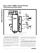
Figure 6. Using the MAX5180/MAX5183 for I/Q Signal Reconstruction