
Datasheet


MAX5170/MAX5172
Low-Power, Serial, 14-Bit DACs
with Voltage Output
______________________________________________________________________________________ 13
Applications Information
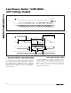
Unipolar Output
Figure 6 shows the MAX5170/MAX5172 configured for
unipolar, rail-to-rail operation with a gain of +1.638V/V.
Table 2 lists the codes for unipolar output voltages. The
maximum output voltage is limited to V
DD
. Use the OS pin
to introduce an offset voltage as shown in Figure 7 and
described in the Offset and Buffer Configurations section.
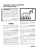
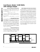
Bipolar Output
Figure 8 shows the MAX5170/MAX5172 configured for
bipolar output operation. The output voltage is given by
the following equation (OS = AGND):
where N represents the numeric value of the DAC’s
binary input code, V
REF
is the voltage of the external
reference. Table 3 shows digital codes and the corre-
sponding output voltage for Figure 8’s circuit.
VV
N
OUT REF
=−
,
2
16 384
1
X
AGNDDGND
MAX5170
MAX5172
DAC
REF
OS
OUT
10k 10k
V-
V+
V
DD
V
OUT
+5V/+3V
Figure 8. Bipolar Output Circuit
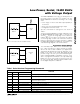
Figure 7. Setting OS for Output Offset
MAX5170
MAX5172
DAC
AGND DGND
REF
OUT
OS
V
OS
+5V/+3V
V
DD
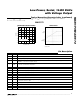
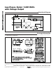
Table 2. Unipolar Code Table
(Circuit of Figure 6)
MAX5170
MAX5172
DAC
REF
OUT
OS
DGNDAGND
+5V/+3V
V
DD
Figure 6. Unipolar Output Circuit (Rail-to-Rail)
Table 3. Bipolar Code Table
(Circuit of Figure 8)
DAC CONTENTS
MSB LSB
ANALOG OUTPUT
+V
REF
[(2 · 16383/16384) - 1]11 1111 1111 1111
10 0000 0000 0001 +V
REF
[(2 · 8193/16384) - 1]
+V
REF
[(2 · 8192/16384) - 1]10 0000 0000 0000
01 1111 1111 1111 +V
REF
[(2 · 8191/16384) - 1]
+V
REF
[(2 · 1/16384) - 1]00 0000 0000 0001
00 0000 0000 0000 -V
REF
ANALOG OUTPUT
+V
REF
(16383/16384) · 1.638
+V
REF
(8193/16384) · 1.638
+V
REF
(8192/16384) · 1.638
+V
REF
(8191/16384) · 1.638
+V
REF
(1/16384) · 1.638
000 0000 0000 0000
00 0000 0000 0001
01 1111 1111 1111
10 0000 0000 0000
10 0000 0000 0001
11 1111 1111 1111
DAC CONTENTS
MSB LSB