
Datasheet

IN to GND (do not exceed
package power dissipation) ...............................-0.3V to +50V
IN to GND (T ≤ 300ms, I
OUT
≤ 250mA) ................ -0.3V to +42V
EN to GND ............................................................-0.3V to +50V
RESET, OUT, OUTSENSE to GND ......................-0.3V to +12V
CT, SET to GND ...................................................-0.3V to +3.5V
IN to OUT ..............................................................-0.3V to +50V
Short-Circuit Duration (V
IN
< 16V) ............................Continuous
Maximum Current into Any Pin (except IN, OUT) ............±20mA
Continuous Power Dissipation (T
A
= +70°C)
TQFN (derate 33.3mW/°C above +70°C)..................2666mW
Thermal Resistance (Note 1):
(θ
JA
, 16-Pin TQFN) ..................................................30.0°C/W
(θ
JC
, 16-Pin TQFN) .......................................................2°C/W
Operating Temperature Range ......................... -40°C to +125°C
Junction Temperature ...................................................... +150°C
Storage Temperature Range ............................ -60°C to +150°C
Lead Temperature (soldering, 10s) .................................+300°C
(V
IN
= 14V, I
OUT
= 1mA, C
IN
= 47µF (low ESR), C
OUT
= 15µF, V
EN
= 2.4V, 10kΩ from RESET to OUT, T
A
= T
J
= -40°C to +125°C,
unless otherwise noted. Typical specifications are at T
A
= +25°C.) (Note 2)
PARAMETER SYMBOL CONDITIONS MIN TYP MAX UNITS
Input Voltage Range V
IN
V
IN
≥ V
OUT
+ 1.5V 6.5 45 V
Supply Current I
Q
Measured at GND,
SET = GND
I
OUT
= 0 70 115
µA
I
OUT
= 250mA 1250
Shutdown Supply Current I
SHDN
V
EN
≤ 0.4V 13 21 µA
REGULATOR
Guaranteed Output Current I
OUT
V
IN
= 6.5V, V
OUT
= 5.0V 250 mA
Output Voltage (Note 3) V
OUT
SET = GND,
5V Version
6.5V ≤ V
IN
≤ 25V,
5mA ≤ I
OUT
≤ 250mA
4.85 5 5.15
V
6.5V ≤ V
IN
≤ 45V,
5mA ≤ I
OUT
≤ 100mA
4.85 5 5.15
SET = GND,
3.3V version
6.5V ≤ V
IN
≤ 25V,
5mA ≤ I
OUT
≤ 250mA
3.217 3.3 3.392
6.5V ≤ V
IN
≤ 45V,
5mA ≤ I
OUT
≤ 100mA
3.217 3.3 3.392
I
OUT
= 5mA, adjustable range 2.5 11.0
Dropout Voltage (Note 4) ∆V
DO
I
OUT
= 250mA, V
OUT
= 5V 0.9 2.2 V
Startup Response
Time (Note 5)
Rising edge of V
IN
to V
OUT
,
R
L
= 500Ω, SET = GND
400 µs
Line Regulation
∆V
OUT
/
∆V
IN
6.5V ≤ V
IN
≤ 45V
5V version -1 +1
mV/V
3.3V version -0.5 +0.8
Enable Voltage V
EN
V
EN
= high, regulator on 2.4
V
V
EN
= low, regulator off 0.4
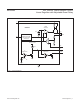
MAX5086 45V, 250mA, Low-Quiescent-Current
Linear Regulator with Adjustable Reset Delay
www.maximintegrated.com
Maxim Integrated
│
2
Note 1: Package thermal resistances were obtained using the method described in JEDEC specification JESD51-7, using a four-layer
board. For detailed information on package thermal considerations, refer to www.maximintegrated.com/thermal-tutorial.
Absolute Maximum Ratings
Stresses beyond those listed under “Absolute Maximum Ratings” may cause permanent damage to the device. These are stress ratings only, and functional operation of the device at these
or any other conditions beyond those indicated in the operational sections of the specifications is not implied. Exposure to absolute maximum rating conditions for extended periods may affect
device reliability.
Electrical Characteristics