
Datasheet


MAX503
5V, Low-Power, Parallel-Input,
Voltage-Output, 10-Bit DAC
______________________________________________________________________________________ 13
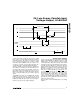
A0 = A1 = 0
A0 = A1 = 1
DAC UPDATE
NBH
NBL & NBM
CS
WR
LDAC = 0 (DAC LATCH IS TRANSPARENT)
Figure 8b. 8-Bit and 16-Bit µP Timing Sequence with LDAC = 0
Figure 5 shows the circuit configuration for a 4-bit µP
application. Figure 6 shows the corresponding timing
sequence. The 4 low bits (S0, S1, D0, D1) are connect-
ed in parallel to the other 4 bits (D2–D5) and then to the
µP bus. Address lines A0 and A1 enable the input data
latches for the high, middle, or low data nibbles. The µP
sends chip select (CS) and write (WR) signals to latch
in each of three nibbles in three cycles when the data is
valid.
Figure 7 shows a typical interface to an 8-bit or a 16-bit
µP. Connect 8 data bits from the data bus to pins S0,
S1, and D0–D5 on the MAX503. With LDAC held high,
the user can load NBH or NBL + NBM in any order.
Figure 8a shows the corresponding timing sequence.
For fastest throughput, use Figure 8b’s sequence.
Address lines A0 and A1 are tied together and the DAC
is loaded in 2 cycles as 8 + 4. In this scheme, with
LDAC held low, the DAC latch is transparent. Always
load NBL and NBM first, followed by NBH.
LDAC is asynchronous with respect to WR. If LDAC is
brought low before or at the same time WR goes high,
LDAC must remain low for at least 50ns to ensure the
correct data is latched. Data is latched into DAC regis-
ters on LDAC’s rising edge.
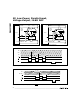
Unipolar Configuration
The MAX503 is configured for a 0V to V
REFIN
unipolar
output range by connecting ROFS and RFB to VOUT
(Figure 9). The converter operates from either single or
dual supplies in this configuration. See Table 3 for the
DAC-latch contents (input) vs. the analog VOUT (output).
In this range, 1LSB = V
REFIN
(2
-10
).
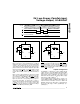
A 0V to 2V
REFIN
unipolar output range is set up by con-
necting ROFS to AGND and RFB to VOUT (Figure 10).
Table 4 shows the DAC-latch contents vs. VOUT. The
MAX503 operates from either single or dual supplies in
this mode. In this range, 1LSB = (2)(V
REFIN
)(2
-10
) =
(V
REFIN
)(2
-9
).
33µF
REFIN
REFOUT
AGND
DGND
REFGND
V
DD
V
SS
ROFS
RFB
VOUT
V
OUT
0V TO -5V
+5V
G = 1
MAX503
33µF
REFIN
REFOUT
AGND
DGND
REFGND
V
DD
V
SS
ROFS
RFB
VOUT
V
OUT
0V TO -5V
+5V
G = 2
MAX503
Figure 9. Unipolar Configuration (0V to +2.048V Output) Figure 10. Unipolar Configuration (0V to +4.096V Output)