
Datasheet


MAX5025–MAX5028
500kHz, 36V Output, SOT23,
Step-Up DC-DC Converters
______________________________________________________________________________________ 11
trace lengths to reduce stray capacitance, trace resis-
tance, and radiated noise. The trace between the out-
put voltage-divider (MAX5025/MAX5026) and the FB
pin must be kept short, as well as the trace between
GND and PGND.
Inductor Layout
The shielded drum type inductors have a small air gap
around the top and bottom periphery. The incident fring-
ing magnetic field from this air gap to the copper plane
on the PC board tends to reduce efficiency. This is a
result of the induced eddy currents on the copper plane.
To minimize this effect, avoid laying out any copper
planes under the mounting area of these inductors.
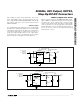
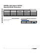
30V Boost Application Circuit
Figures 2 and 3 show the MAX5025/MAX5026 operat-
ing in a 30V boost application. Figure 3 has an RC filter
to reduce noise at the output. These circuits provide
output currents greater than 4mA with an input voltage
of 5V or greater. They are designed by following the
Design Procedure
section. Operating characteristics of
these circuits are shown in the
Typical Operating
Characteristics
section.
V
CC
V
OUT
+30V
GND
FB
PGND
C1
4.7μF
C2
1μF
LX
L1
47μH
MAX5025
MAX5026
C2
1μF
V
CC
= 4.5V TO 11V
(MAX5025)
V
CC
= 3V TO 11V
(MAX5026)
D1
R1
147kΩ
R2
6.34kΩ
TOKO 47μH INDUCTOR
A915BY-470M
ZETEX SCHOTTKY DIODE
ZHCS500
SHDN
Figure 2. Adjustable 30V Output Circuit
V
CC
V
OUT
+30V
GND
FB
PGND
C1
4.7μF
C2
1μF
LX
L1
47μH
MAX5025
MAX5026
C3
1μF
V
CC
= 4.5V TO 11V
(MAX5025)
V
CC
= 3V TO 11V
(MAX5026)
D1
R1
147kΩ
R3
100Ω
R2
6.34kΩ
TOKO 47μH INDUCTOR
A915BY-470M
ZETEX SCHOTTKY DIODE
ZHCS500
SHDN
Figure 3. Adjustable 30V Output Circuit with RC Filter