
Datasheet


MAX5025–MAX5028
500kHz, 36V Output, SOT23,
Step-Up DC-DC Converters
10 ______________________________________________________________________________________
For a design in which V
IN
= 5V, V
OUT
= 30V, I
OUT
=
4mA, η = 0.5, and T
S
= 2µs,
L
UPPER
= 87µH
and
L
LOWER
= 12µH.
For a worst-case scenario in which V
IN
= 4.75V, V
OUT
= 29V, I
OUT
= 4.4mA, η = 0.5, and T
S
= 1.25µs,
L
UPPER
= 46µH
and
L
LOWER
= 9µH.
The choice of 47µH as the recommended inductance
value is reasonable given the worst-case scenario
above. In general, the higher the inductance, the lower
the switching noise. Load regulation is also better with
higher inductance.
Diode Selection
The MAX5025–MAX5028’s high switching frequency
demands a high-speed rectifier. Schottky diodes are
recommended for most applications because of their
fast recovery time and low forward-voltage drop.
Ensure that the diode’s peak current rating is greater
than or equal to the peak inductor current. Also, the
diode reverse breakdown voltage must be greater than
V
OUT
. Table 2 lists diode vendors.
Capacitor Selection
Output Filter Capacitor
The output filter capacitor should be 1µF or greater. To
achieve low output ripple, a capacitor with low ESR, low
ESL, and high capacitance value should be selected.
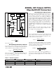
For very low output ripple applications, the output of the
boost converter can be followed by an RC filter to fur-
ther reduce the ripple. Figure 3 shows a 100Ω, 1µF fil-
ter used to reduce the switching output ripple to
1mVp-p.
X7R ceramic capacitors are better for this boost appli-
cation because of their low ESR and tighter tolerance
over temperature than the Y5V ceramic capacitors.
Table 3 below lists manufacturers of recommended
capacitors.
Input Capacitor
Bypass V
CC
with a 4.7µF ceramic capacitor as close to
the IC as is practical.
Applications Information
Layout Considerations
The MAX5025–MAX5028 switch at high speed, man-
dating careful attention to layout for optimum perfor-
mance. Protect sensitive analog grounds by using a
star ground configuration. Minimize ground noise by
connecting GND, PGND, the input bypass-capacitor
ground lead, and the output-filter ground lead to a sin-
gle point (star ground configuration). Also, minimize
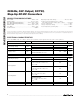
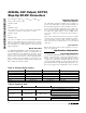
Table 2. Schottky Diode Vendors
VENDOR PHONE FAX PART NUMBERS
Comchip 510-657-8671 510-657-8921 CDBS1045
Panasonic 408-942-2912 408-946-9063 MA2Z785
ST-Microelectronics 602-485-6100 602-486-6102 TMMBAT48
Vishay-Telefunken 402-563-6866 402-563-6296 BAS382
Zetex 631-360-2222 631-360-8222 ZHCS500
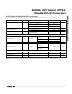
Table 3. Capacitor Table
COMPANY PHONE FAX PART NUMBERS
GRM42-2X7R105K050AD (1µF capacitor)
Murata 814-237-1431 814-238-0490
GRM32-1210R71C475R (4.7µF capacitor)
UMK325BJ105KH (1µF capacitor)
Taiyo Yuden 408-573-4150 408-573-4159
EMK316BJ475ML (4.7µF capacitor)
C3225X7R1H155K (1.5µF capacitor)
TDK 847-803-6100 847-803-6296
C3225X7R1H105K (1µF capacitor)