
Datasheet


Dual/Quad, Unipolar/Bipolar,
High-Voltage Digital Pulsers
MAX4940/MAX4940A
12 _____________________________________________________________________________________
Exposed Pad and Layout Concerns
The MAX4940/MAX4940A provide an exposed pad
(EP) underneath the TQFN package for improved ther- ther-ther-
mal performance. EP is internally connected to V
NN1
.
Connect EP to V
NN1
externally. To aid heat dissipation,
connect EP to a similarly sized pad on the component
side of the PCB. This pad should be connected through
the solder-side copper by several plated holes to a large
heat spreading copper area to conduct heat away from
the device.
The MAX4940/MAX4940A high-speed pulsers require low-
inductance bypass capacitors to their supply inputs. High-
speed PCB trace design practices are recommended. Pay
particular attention to minimize trace lengths and use suf- minimize trace lengths and use suf-minimize trace lengths and use suf- lengths and use suf-lengths and use suf-
ficient trace width to reduce inductance. Use of surface-
mount components is recommended.
Supply Sequencing
In a typical trilevel application when V
NN1
and V
NN2
are externally shorted (V
NN1
= V
NN2
), the MAX4940/
MAX4940A do not require any power sequencing. In
general, and in particular for the multilevel applica-
tion, V
NN1
must be less than or equal to V
NN2
(V
NN1
P
V
NN2
) at all times. No other power-supply sequencing is
required for the MAX4940/MAX4940A.
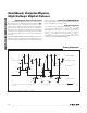
Timing Diagrams
Figure 1. Detail Timing (R
L
= 100I, C
L
= 100pF)
50%
10%
90%
10%
90%
10%
90%
10%
10% 10%
50%50% 50%
50%50%50%
90% 90%
50%
t
POH
t
RNP
t
PHO
t
FPO
t
ROP
t
FON
t
RNO
t
PLO
t
POL
t
PHL
t
PLH
t
FPN
OUT_
INP_
INN_
CLP_ = HIGH
GND
GND
V
DD
V
PP_
V
NN_