
Datasheet


Dual/Quad, Unipolar/Bipolar,
High-Voltage Digital Pulsers
MAX4940/MAX4940A
______________________________________________________________________________________ 11
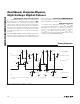
Active Clamps
The MAX4940/MAX4940A feature an integrated active
clamp circuit to improve pulse quality and reduce 2nd
harmonic distortion. The clamp circuit consists of an
n-channel (DC-coupled) and a p-channel (DC-coupled)
high-voltage FETs that are switched on or off by the logic
clamp input (CLP_).
The MAX4940/MAX4940A feature protected clamp devic-
es, allowing the clamp circuit to be used in bipolar pulsing
circuits (see Figures 3 and 4). A diode in series with the
OUT_ output prevents the body diode of the low-side FET
from turning on when a voltage lower than GND is pres-
ent. Another diode in series with the OUT_ output prevents
the body diode of the high-side FET from turning on when
a voltage higher than ground is present. The MAX4940/
MAX4940A have an active clamp on all outputs.
For the MAX4940 only, the user can connect the active
clamp input (CLP_) to a logic-high voltage and drive
only the INP_ and INN_ inputs to minimize the number of
signals used to drive the device. In this case, whenever
both the INP_ and INN_ inputs are low and the CLP_
input is high, the active clamp circuit pulls the output to
GND (see the Truth Tables section for more information).
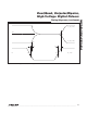
Integrated Blocking Diodes
(MAX4940A Only)
The high-voltage OUT2A/OUT2B outputs of the
MAX4940A feature integrated blocking diodes that allow
the user to implement multilevel pulsing by connect-
ing the outputs of multiple pulser channels in parallel.
Internal diodes in series with the OUT2A and OUT2B
outputs prevent the body diode of the high-side and low-
side FETs from switching on when a voltage greater than
V
NN2
or V
PP2
is present on the output (see Figure 4).
Thermal Protection
A thermal shutdown circuit with a typical threshold of
+155NC prevents damage due to excessive power dis- power dis-power dis-
sipation. When the junction temperature exceeds T
J
=
+155NC, all outputs are disabled. Normal operation typi- Normal operation typi-Normal operation typi-
cally resumes after the IC’s junction temperature drops
below +130NC.
Applications Information
AC-Coupling Capacitor Selection
The value of all AC-coupling capacitors (between C
DP_
and C
GP_
, and between C
DN_
and C
GN_
) should be
between 1nF to 10nF. The voltage rating of the capacitor
should be greater than V
PP_
and V
NN_
. The capacitors
should be placed as close as possible to the device.
Power Dissipation
The power dissipation of the MAX4940/MAX4940A con-
sists of three major components caused by the current
consumption from V
CC
, V
PP_
, and V
NN_
. The sum of
these components (P
VCC
, P
VPP_
, and P
VNN_
) must be
kept below the maximum power-dissipation limit. See
the Typical Operating Characteristics section for more
information on typical supply currents versus switching
frequencies.
The device consumes most of the supply current from
V
CC
supply to charge and discharge internal nodes
such as the gate capacitance of the high-side FET (C
P
)
and the low-side FET (C
N
). Neglecting the small quies-
cent supply current and a small amount of current used
to charge and discharge the capacitances at the internal
gate clamp FETs, the power consumption can be esti-
mated as follows:
( ) ( )
( )
2 2
VCC N CC IN P CC IN
IN INN_ INP_
P C V f C V f BRF BTD
f f f
= × × + × × × ×
= +
where f
INN_
and f
INP_
are the switching frequency of
the inputs INN_, INP_, respectively, and where BRF is
the burst response frequency, and BTD is the burst time
duration. The typical values of the gate capacitances are
C
N
= 1.2FF, C
P
= 0.4FF.
See the Typical Operating Characteristics for V
PP_
and
V
NN_
power consumption.
Power Supplies and Bypassing
The MAX4940/MAX4940A operate from independent
supply voltage sets (only V
DD
, V
CC
, and V
EE
are com-
mon to all channels). V
PP1
/V
NN1
supply two channels
and V
PP2
/V
NN2
supply the other two channels. The logic
input circuit operates from a +2.37V to +6V single sup-
ply (V
DD
). The level-shift driver dual supplies, V
CC
/V
EE
operate from Q4.75V to Q12.6V.
The V
PP_
/V
NN_
high-side and low-side supplies are
driven from a single positive supply up to +220V, from a
single negative supply up to -220V, or from Q110V dual
supplies. Either V
PP_
or V
NN_
can be set at 0. Bypass
each supply input to ground with a 0.1FF capacitor as
close as possible to the device.
Depending on the applications, additional bypassing may
be needed to maintain the input of both V
NN_
and V
PP_
stable during output transitions. For example, with C
OUT
= 100pF and R
OUT
= 100I load, the use of an additional
10FF (typ) electrolytic capacitor is recommended.