
Datasheet


MAX4906/MAX4606F/MAX4907/MAX4907F
High-/Full-Speed USB 2.0 Switches
4 _______________________________________________________________________________________
ELECTRICAL CHARACTERISTICS (continued)
(V+ = +3V to +3.6V, T
A
= T
MIN
to T
MAX
, unless otherwise noted. Typical values are at V+ = 3.3V, T
A
= +25°C.) (Note 2)
PARAMETER
SYMBOL
CONDITIONS
MIN TYP MAX
UNITS
Total Harmonic Distortion Plus
Noise
THD+N
V
COM_
= 2V
P-P
, R
L
= 600Ω, f = 20Hz to
20kHz
0.03
%
Charge Injection Q
V
GEN
= 1.5V, R
GEN
= 0Ω, C
L
= 100pF,
Figure 6
5pC
SWITCH LOGIC
Logic-Input-Voltage Low V
IL
0.4 V
Logic-Input-Voltage High V
IH
1.1 V
Input-Logic Hysteresis V
HYST
100
mV
Input Leakage Current I
IN
V+ = 3.6V, V
IN
= 0 or V+ -1 +1 µA
Operating Supply-Voltage Range
V+ 3.0 3.6 V
Quiescent Supply Current I+
V+ = 3.6V, V
IN
= 0 or V+, SHDN or
SHDN/EN = 0
120
300 µA
Quiescent Supply Current During
Shutdown
I+
V+ = 3.6V, V
IN
= 0 or V+, SHDN or
SHDN/EN = V+
2µA
Note 2: All units are 100% production tested at T
A
= +25°C. Limits over the operating temperature range are guaranteed by design
and not production tested.
Note 3: The switch will turn off for voltages above (V
FP
); therefore, protecting downstream circuits in case of a fault condition
(MAX4906F/MAX4907F).
Note 4: ΔR
ON(MAX)
= | R
ON(CH1) –
R
ON(CH2)
|
Note 5: Flatness is defined as the difference between the maximum and minimum value of on-resistance, as measured over
specified analog signal ranges.
Note 6: Between any two switches.
Note 7: Switch off-capacitance, switch on-capacitance, output skew between switches, and output skew same-switch limits are not
production tested; design guaranteed by bench characterization.
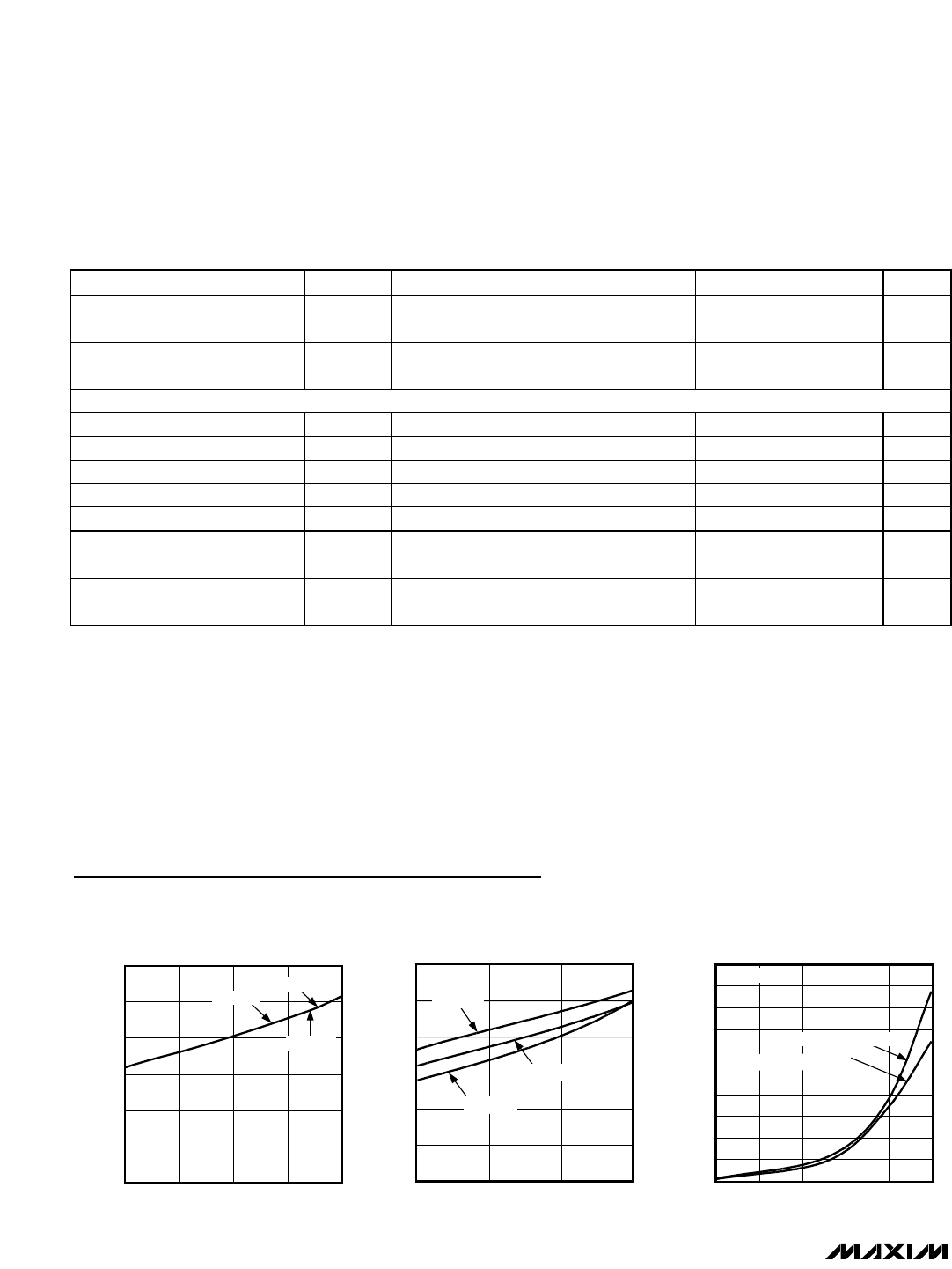
Typical Operating Characteristics
(T
A
= +25°C, unless otherwise noted.)
0
1500
1000
500
2000
2500
3000
3500
4000
4500
5000
-40 10-15 35 60 85
LEAKAGE CURRENT vs. TEMPERATURE
MAX4906 toc03
TEMPERATURE (°C)
LEAKAGE CURRENT (pA)
COM ON-LEAKAGE
COM OFF-LEAKAGE
V+ = 3.6V
0
2
1
4
3
5
6
01.80.9 2.7 3.6
ON-RESISTANCE vs. V
COM
MAX4906 toc01
V
COM
(V)
R
ON
(Ω)
V+ = 3.3V
V+ = 3.0V
V+ = 3.6V
0
2
1
4
3
5
6
0 1.1 2.2 3.3
MAX4906 toc02
V
COM
(V)
ON-RESISTANCE vs. V
COM
R
ON
(Ω)
T
A
= +40
°
C
T
A
= +25
°
C
T
A
= +85
°
C
V+ = 3.3V