
Datasheet


MAX4800A/MAX4802A
Low-Charge-Injection, 8-Channel, High-Voltage
Analog Switches with 20MHz Serial Interface
_______________________________________________________________________________________ 5
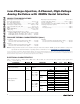
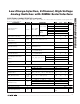
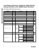
TIMING CHARACTERISTICS
(V
DD
= +2.7V to +6V, V
PP
= +40V to (V
NN
+ 200V), V
NN
= -40V to -160V, T
A
= T
MIN
to T
MAX
, unless otherwise noted. Typical values
are at T
A
= +25°C.) (Note 2)
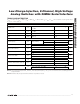
PARAMETER SYMBOL CONDITIONS MIN TYP MAX UNITS
ANALOG SWITCH
Turn-On Time t
ON
V
NO_
= V
PP
- 10V, R
L
= 10kΩ, V
NN
= -40V
to -160V
5µs
Turn-Off Time t
OFF
V
NO_
= V
PP
- 10V, R
L
= 10kΩ, V
NN
= -40V
to -160V
5µs
Output Switching Frequency f
SW
Duty cycle = 50% 50 kHz
Maximum V
COM_
, V
NO_
Slew
Rate
dV/dt (Note 4) 20 V/ns
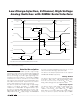
LOGIC TIMING (Figure 1)
V
DD
= +5V ±10% 20
CLK Frequency f
CLK
D ai sy chai ni ng
V
DD
= +3V ±10% 10
MHz
V
DD
= +5V ±10% 10
DIN to CLK Setup Time t
DS
V
DD
= +3V ±10% 16
ns
V
DD
= +5V ±10% 3
DIN to CLK Hold Time t
DH
V
DD
= +3V ±10% 3
ns
V
DD
= +5V ±10% 36
CLK to LE Setup Time t
CS
V
DD
= +3V ±10% 65
ns
V
DD
= +5V ±10% 14
LE Low Pulse Width t
WL
V
DD
= +3V ±10% 22
ns
V
DD
= +5V ±10% 20
CLR High Pulse Width t
WC
V
DD
= +3V ±10% 40
ns
V
DD
= +5V ±10% 50
CLK Rise and Fall Times (Note 4) t
R
, t
F
V
DD
= +3V ±10% 50
ns
V
DD
= +5V ±10%, C
L
≤ 20pF 6 42
CLK to DOUT Delay t
DO
V
DD
= +3V ±10%, C
L
≤ 20pF 12 80
ns
Note 2: Specifications at 0°C are guaranteed by correlation and design.
Note 3: The analog-signal input V
COM_
and V
NO_
must satisfy V
NN
≤ (V
COM_
, V
NO_
) ≤ V
PP
, or remain unconnected during power-up
and power-down.
Note 4: Guaranteed by design and characterization; not production tested.