
Datasheet


MAX4731/MAX4732/MAX4733
50
Ω,
Dual SPST Analog Switches in UCSP
_______________________________________________________________________________________ 5
Note 3: The algebraic convention, where the most negative value is a minimum and the most positive value a maximum, is used in
this data sheet.
Note 4: UCSP and TDFN parts are 100% tested at +25°C only, and guaranteed by design over temperature. µMAX parts are
100% tested at +85°C and +25°C and guaranteed by design over temperature.
Note 5: ∆R
ON
= R
ON(MAX)
- R
ON(MIN)
.
Note 6: UCSP on-resistance matching between channels and on-resistance flatness guaranteed by design.
Note 7: Flatness is defined as the difference between the maximum and minimum value of on-resistance as measured over the
specified analog signal range.
Note 8: Guaranteed by design.
Note 9: Off-Isolation = 20 log
10
(V
NO_
/V
COM_
), V
NO_
= output, V
COM_
= input to off switch.
Note 10: Between any two switches.
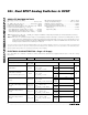
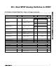
ELECTRICAL CHARACTERISTICS—Single +5V Supply
(V+ = +5V ±10%, V
IH
= +2.0V, V
IL
= +0.8V, T
A
= T
MIN
to T
MAX
, unless otherwise noted. Typical values are at V+ = +5V, T
A
= +25°C.)
(Notes 3, 4)
PARAMETER
SYMBOL
CONDITIONS T
A
MIN
TYP
MAX
UNITS
Crosstalk (Note 10) V
CT
f = 1MHz, V
COM_
= 1V
RMS
,
R
L
= 50Ω, C
L
= 5pF,
Figure 6
+25°C -108
dB
NO_ or NC_ Off-Capacitance C
OFF
f = 1MHz, Figure 7
+25°C
20 pF
COM_ Off-Capacitance
C
COM_
(
OFF
)
f = 1MHz, Figure 7
+25°C
20 pF
COM_ On-Capacitance
C
COM_
(
ON
)
f = 1MHz, Figure 7
+25°C
40 pF
LOGIC INPUT
Input Logic High V
IH
2.0 V
Input Logic Low V
IL
0.8 V
Input Leakage Current I
IN
V
IN_
= 0V or V+ -1
+0.005
+1 µA
SUPPLY
Power-Supply Range V+ 2.0 11 V
Positive Supply Current I+
V+ = +5.5V, V
IN_
= 0V or V+,
all switches on or off
0.0001
1µA