
Datasheet


MAX4649
45Ω, SPDT Analog Switch in SOT23-8
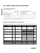
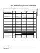
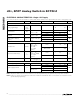
4 _______________________________________________________________________________________
ELECTRICAL CHARACTERISTICS—Single +12V Supply
(V+ = +12V, V- = 0, V
IH
= 2.4V, V
IL
= 0.8V, T
A
= T
MIN
to T
MAX
, unless otherwise noted. Typical values are at T
A
= +25°C.) (Notes 2, 3)
PARAMETER SYMBOL CONDITIONS T
A
MIN TYP MAX UNITS
ANALOG SWITCH
Analog Signal Range
V
NO
,
V
NC
,
V
COM
0V+V
+25°C6890
On-Resistance R
ON
I
COM
= 1mA; V
NO
or V
NC
= +10V
T
MIN
to T
MAX
115
Ω
+25°C 0.7 6
On-Resistance Matching Between
Channels
∆R
ON
I
COM
= 1mA; V
NO
or V
NC
= +10V
T
MIN
to T
MAX
7
Ω
+25°C917
On-Resistance Flatness
(Note 4)
R
FL AT
(
ON
)
I
COM
= 1mA; V
NO
or V
NC
= +2V, +6V,
+10V
T
MIN
to T
MAX
23
Ω
DYNAMIC
+25°C 116 165
Transition Time t
TRANS
V
NO
or V
NC
= 0,
10V or 10V, 0;
R
L
= 1kΩ;
C
L
= 35pF;
Figure 2
T
MIN
to T
MAX
200
ns
+25°C136
Break-Before-Make Delay t
D
V
NO
or V
NC
=
+10V; R
L
= 300Ω;
C
L
= 35pF;
Figure 3
T
MIN
to T
MAX
1
ns
Charge Injection Q
V
GE N
= 0; R
GE N
= 0;
C
L
= 1nF; Figure 4
+25°C1pC
POWER SUPPLY
Power Supply Range 936V
+25°C2240
V
IN
= +5V
T
MIN
to T
MAX
50
+25°C 0.01 1
Positive Supply Current I+
V
IN
= 0 or V+
T
MIN
to T
MAX
10
µA
Note 2: The algebraic convention is used in this data sheet; the most negative value is shown in the minimum column.
Note 3: All parts are 100% tested at +25°C. Limits across the full temperature range are guaranteed by design and correlation.
Note 4: Flatness is defined as the difference between the maximum and minimum value of on-resistance as measured over the
specified analog signal range.