
Datasheet


MAX4649
45Ω, SPDT Analog Switch in SOT23-8
2 _______________________________________________________________________________________
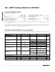
ABSOLUTE MAXIMUM RATINGS
ELECTRICAL CHARACTERISTICS—Dual ±15V Supplies
(V+ = +15V, V- = -15V, V
IH
= 2.4V, V
IL
= 0.8V, T
A
= T
MIN
to T
MAX
, unless otherwise noted. Typical values are at T
A
= +25°C.) (Notes
2, 3)
Stresses beyond those listed under “Absolute Maximum Ratings” may cause permanent damage to the device. These are stress ratings only, and functional
operation of the device at these or any other conditions beyond those indicated in the operational sections of the specifications is not implied. Exposure to
absolute maximum rating conditions for extended periods may affect device reliability.
V+ ........................................................................-0.3V to +44.0V
V- .........................................................................-44.0V to +0.3V
V+ to V-................................................................-0.3V to +44.0V
All Other Pins (Note 1) ..........................(V- - 0.3V) to (V+ + 0.3V)
Continuous Current into any Terminal ..............................±10mA
Continuous Current (COM, NO, NC) ................................±30mA
Peak Current (COM, NO, NC)
(pulsed at 1ms, 10% duty cycle)..................................±60mA
Continuous Power Dissipation (T
A
= +70°C)
8-Pin SOT23 (derate 8.9mW/°C above +70°C)...........714mW
Operating Temperature Range
MAX4649EKA ............................................-40°C to +85°C
Storage Temperature Range .............................-65°C to +150°C
Junction Temperature......................................................+150°C
Lead Temperature (soldering, 10s) .................................+300°C
Note 1: Signals on NO, NC, COM, or IN exceeding V+ or V- are clamped by internal diodes. Limit forward-diode current to maxi-
mum current rating.
PARAMETER SYMBOL CONDITIONS T
A
MIN TYP MAX UNITS
ANALOG SWITCH
Analog Signal Range
V
NO
,
V
NC
,
V
COM
V- V+ V
+25°C3345
On-Resistance R
ON
I
COM
= 1mA; V
NO
or
V
NC
= ±10V
T
MIN
to T
MAX
60
Ω
+25°C 0.6 5
On-Resistance Matching Between
Channels
∆R
ON
I
COM
= 1mA; V
NO
or
V
NC
= ±10V
T
MIN
to T
MAX
6
Ω
+25°C 1.5 7
On-Resistance Flatness
(Note 4)
R
FLAT
(ON)
I
COM
= 1mA; V
NO
or
V
NC
= +5V, 0, -5V
T
MIN
to T
MAX
10
Ω
+25°C -2 0.01 2
NO or NC Off-Leakage
Current
I
NO(OFF)
or
I
NC
(
OFF
)
V
COM
= -14V, +14V;
V
NO
or V
NC
= +14V,
-14V
T
MIN
to T
MAX
-10 10
nA
+25°C-4 4
COM On-Leakage
Current
I
COM
(
ON
)
V
COM
= +14V, -14V;
V
NO
or V
NC
= +14V,
-14V or floating
T
MIN
to T
MAX
-20 20
nA
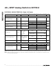
DIGITAL I/O
Input Logic High Voltage V
IH
2.4 V
Input Logic Low Voltage V
IL
0.8 V
Input Leakage I
IN
V
IN
= 0 or +5V -1 1 µA
(Voltages referenced to GND.)