
Datasheet


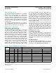


Note: Input and output pins are identical and interchangeable. Any may be considered an input or output; signals pass equally well
in both directions.
PIN
NAME FUNCTION
MAX4581L MAX4582L MAX4583L
SO/QSOP QFN SO/QSOP QFN SO/QSOP QFN
1, 2, 4, 5,
12–15
2, 3,
10–13,
15, 16
— — — — X0–X7 Analog Switch Inputs 0–7
3 1 13 11 14 12 X Analog Switch X Output
6 4 6 4 6 4 Enable
Digital Enable Input. Drive enable low or
connect to GND for normal operation.
7, 8 5, 6 7, 8 5, 6 7, 8 5, 6 GND
Ground. Connect to digital ground. (Analog
signals have no ground reference; they are
limited to V
CC
.)
9 7 — — 9 7 C Digital Address C Input
10 8 9 7 10 8 B Digital Address B Input
11 9 10 8 11 9 A Digital Address A Input
16 14 16 14 16 14 VCC
Positive Analog and Digital Supply Voltage
Input. Bypass with a 0.1µF capacitor to GND.
— —
11, 12,
14, 15,
9, 10,
12, 13
— — X0–X3 Analog Switch X Inputs 0–3
— — 1, 2, 4, 5
2, 3,
15, 16
— — Y0–Y3 Analog Switch Y Inputs 0–3
— — 3 1 15 13 Y Analog Switch Y Output
— — — — 13 11 X1 Analog Switch X Normally Open Input
— — — — 12 10 X0 Analog Switch X Normally Closed Input
— — — — 1 15 Y1 Analog Switch Y Normally Open Input
— — — — 2 16 Y0 Analog Switch Y Normally Closed Input
— — — — 3 1 Z1 Analog Switch Z Normally Open Input
— — — — 5 3 Z0 Analog Switch Z Normally Closed Input
— — — — 4 2 Z Analog Switch Z Output
— EP — EP — EP
Exposed
Pad
Bottom of QFN package only. Contains
an exposed pad that must be connected
externally to V
CC
.
MAX4581L/MAX4582L/
MAX4583L
Low-Voltage, CMOS Analog
Multiplexers/Switches
www.maximintegrated.com
Maxim Integrated
│
6
Pin Description