
Datasheet


Detailed Description
The MAX4524L/MAX4525L are low-voltage, single-sup-
ply CMOS analog switches that operate from a single
supply of +2V to +12V. Operation with a +12V supply opti-
mizes the performance by reducing their on-resistance
to 100Ω. The MAX4524L is configured as a 4-channel
multiplexer/demultiplexer and the MAX4525L is a double-
pole/double-throw (DPDT) switch. These devices have an
inhibit input (INH) to simultaneously open all signal paths.
Each switch can handle rail-to-rail analog signals. The
off-leakage current is typically only 0.1nA at +25°C and
10nA (max) over temperature. All digital inputs have 0.8V
to 2.0V logic-level thresholds, ensuring TTL/CMOS-logic
compatibility when using a single +12V supply.
Applications Information
Power-Supply Considerations
The MAX4524L/MAX4525Ls’ construction is typical of
most CMOS analog switches. The supply input, V+, is
used to power the internal CMOS switches and set the
limits of the analog voltage on any switch. Reverse ESD
protection diodes are internally connected between each
analog signal pin and both V+ and GND. If any analog
signal exceeds V+ or goes below GND, one of these
diodes conducts. During normal operation, these reverse-
biased ESD diodes leak, forming the only current drawn
from V+ or GND. Virtually all the analog leakage current
comes from the ESD diodes. Although the ESD diodes
on a given signal pin are identical, and therefore fairly
well balanced, they are reverse biased differently. Each is
biased by either V+ or GND and the analog signal. This
means that leakage varies as the signal varies. The differ-
ence in the two diode leakages to the V+ and GND pins
constitutes the analog signal-path leakage current. All
analog leakage current flows between each pin and one
of the supply terminals, not to the other switch terminal.
This is why both sides of a given switch can show leakage
currents of either the same or opposite polarity.
There is no connection between the analog signal paths
and GND. V+ and GND power the internal logic and logic-
level translators, and set both the input and output logic
limits. The logic-level translators convert the logic levels
into switched V+ and GND signals to drive the gates of
the analog signals. This drive signal is the only connection
between the logic supplies (and signals) and the analog
supplies.
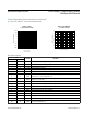
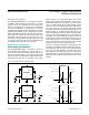
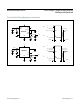
Figure 1. Inhibit Switching Times
50%
t
OFF
V+
0V
V
NO0
V
OUT
V
INH
0V
90%
90%
t
ON
50%
t
OFF
V+
0V
V
NO_
V
OUT
V
INH
0V
90%
90%
t
ON
V
INH
V
INH
V+
V
OUT
GND
V+
ADDB
ADDA
INH
NO0
NO1–NO3
COM
V+
MAX4524L
300W
50W
35pF
V+
V
OUT
GND
V+
ADD
INH
NO_
NC_
COM_
V+
MAX4525L
300W
35pF
50W
MAX4524L/MAX4525L Low-Voltage, Single-Supply Analog
Multiplexers/Switches
www.maximintegrated.com
Maxim Integrated
│
6
Test Circuits/Timing Diagrams