
Datasheet


(V+ = 12V, V
INH
= GND, T
A
= +25°C, unless otherwise noted.)
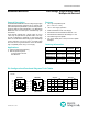
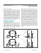
PIN
NAME FUNCTION
MAX4524L MAX4525L
1 — NO2 Analog Switch Normally Open Input 2
— 1 NOA Analog Switch A Normally Open Input
2 — NO3 Analog Switch Normally Open Input 3
— 2 COMA Analog Switch A Common
3 — NO1 Analog Switch Normally Open Input 1
— 3 NCA Analog Switch A Normally Closed Input
4 4 INH
Inhibit. Drive INH low or connect to GND for normal operation. Drive INH high or
connect to V+ to turn all switches off.
5 5 GND
Ground. Connect to digital ground (analog signals have no ground reference, but are
limited to V+ and GND).
6 — ADDB Logic-Level Address Input (see Truth Tables)
— 6 ADD Logic-Level Address Input (see Truth Tables)
7 — ADDA Logic-Level Address Input (see Truth Tables)
— 7 NCB Analog Switch B Normally Closed Input
8 — NO0 Analog Switch Normally Open Input 0
— 8 NOB Analog Switch B Normally Open Input
9 — COM Analog Switch Common
— 9 COMB Analog Switch A Common
10 10 V+ Positive Analog and Digital Supply Voltage. Bypass with a 0.1µF capacitor to GND.
EP EP
Exposed
PAD
The bottom of the IC (TDFN package only) contains an exposed pad that must be
connected externally to V+.
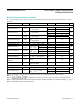
0 62 4 8 10 12
SUPPLY CURRENT
vs. LOGIC-LEVEL VOLTAGE
MAX4524L toc09
V
ADD_
, V
INH
(V)
SUPPLY CURRENT (A)
0.0001
0.01
0.001
0.1
1
10
100
1000
10,000
0
0.4
0.2
1.0
0.8
0.6
1.2
1.4
1.8
1.6
2.0
0 2 31 4 5 6 7 8 9 10 1211
INPUT LOGIC THRESHOLD
vs. SUPPLY VOLTAGE
MAX4524L toc10
SUPPLY VOLTAGE (V)
LOGIC THRESHOLD (V)
MAX4524L/MAX4525L Low-Voltage, Single-Supply Analog
Multiplexers/Switches
Maxim Integrated
│
5
www.maximintegrated.com
Typical Operating Characteristics (continued)
Pin Description