
Datasheet

MAX4321
Low-Cost, Low-Voltage, Rail-to-Rail,
Input/Output, SOT23 5MHz Op Amp
_______________________________________________________________________________________ 9
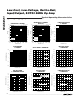
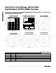
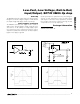
R
S
C
L
MAX4321
Figure 7. Capacitive-Load-Driving Circuit
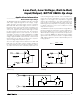
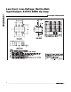
V
OUT
0V TO 2.7V
STEP FOR
POWER-UP
TEST
SUPPLY-CURRENT
MONITORING POINT
V
CC
10Ω2k
10k
2k
MAX4321
Figure 8. Power-Up Test Circuit
Figure 10. Power-Up Supply Current
V
CC
5μs/div
VOLTAGE
1V/div
OUT
Figure 9. Power-Up Output Voltage
V
CC
1V/div
5μs/div
I
CC
500μA/div
Power-Up
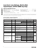
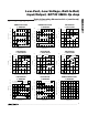
The MAX4321 typically settles within 1µs after power-up.
Using the test circuit of Figure 8, Figures 9 and 10 show
the output voltage and supply current on power-up.
Power Supplies and Layout
The MAX4321 operates from single +2.4V to +6.5V or
dual ±1.2V to ±3.25V supplies, though it typically oper-
ates down to +1.8V (±0.9V). For single-supply opera-
tion, bypass the power supply with a 0.1µF ceramic
capacitor in parallel with at least 1µF. For dual supplies,
bypass each supply to ground.
Good layout improves performance by decreasing the
amount of stray capacitance at the op amp’s inputs
and outputs. To decrease stray capacitance, minimize
trace lengths and resistor leads by placing external
components close to the op amp’s pins.
Package Information
TRANSISTOR COUNT: 84