
Datasheet
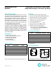

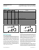

between the output and the capacitive load (Figures 6a, 6b,
6c). Note that this alternative results in a loss of gain accu-
racy because R
ISO
forms a voltage divider with the R
LOAD
.
Power-Supply Bypassing and Layout
The MAX4245/MAX4246/MAX4247 family operates from
either a single +2.5V to +5.5V supply or dual ±1.25V to
±2.75V supplies. For single-supply operation, bypass the
power supply with a 100nF capacitor to V
SS
(in this case
GND). For dual-supply operation, both the V
DD
and the
V
SS
supplies should be bypassed to ground with separate
100nF capacitors.
Good PC board layout techniques optimize performance
by decreasing the amount of stray capacitance at the op
amp?s inputs and output. To decrease stray capacitance,
minimize trace lengths and widths by placing external
components as close to the device as possible. Use
surface-mount components when possible.
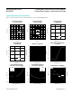
Figure 5. Shutdown Waveform
Figure 6b. Pulse Response Without Isolating Resistor
Figure 6c. Pulse Response With Isolating Resistor
Figure 6a. Using a Resistor to Isolate a Capacitive Load from
the Op Amp
OUT
SHDN
2V/div
2V/div
400µs/div
OUT
IN
100mV/div
100mV/div
10µs/div
R
ISO
= 0Ω
R
L
= 2kΩ
C
L
= 2200pF
OUT
IN
100mV/div
100mV/div
10µs/div
R
ISO
= 100Ω
R
L
= 2kΩ
C
L
= 2200pF
OUT
IN
R
ISO
R
L
C
L
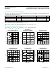
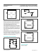
TOP VIEW
V
DD
OUTB
INB-
INB+V
SS
INA+
INA-
OUTA
µMAX
1
2
3
4
10
9
8
7
5 6SHDNA SHDNB
MAX4247
+
MAX4245/MAX4246/
MAX4247
Ultra-Small, Rail-to-Rail I/O with Disable,
Single-/Dual-Supply, Low-Power Op Amps
www.maximintegrated.com
Maxim Integrated
│
9
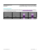
Pin Congurations (continued)
Chip Information
PROCESS: BiCMOS