
Datasheet


Detailed Description
Rail-to-Rail Input Stage
The MAX4245/MAX4246/MAX4247 have rail-to-rail input
and output stages that are specifically designed for low-
voltage, single-supply operation. The input stage consists
of composite NPN and PNP differential stages, which
operate together to provide a common-mode range
extending to both supply rails. The crossover region
of these two pairs occurs halfway between V
DD
and
V
SS
. The input offset voltage is typically ±400µV. Low-
operating supply voltage, low supply current and rail-to-
rail outputs make this family of operational amplifiers an
excellent choice for precision or general-purpose, low-
voltage, battery-powered systems.
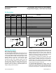
Since the input stage consists of NPN and PNP pairs, the
input bias current changes polarity as the common-mode
voltage passes through the crossover region. Match the
effective impedance seen by each input to reduce the
offset error caused by input bias currents flowing through
external source impedance (Figures 1a and 1b).
The combination of high-source impedance plus input
capacitance (amplifier input capacitance plus stray capac-
itance) creates a parasitic pole that can produce an
underdamped signal response. Reducing input capaci-
tance or placing a small capacitor across the feedback
resistor improves response in this case.
The MAX4245/MAX4246/MAX4247 family’s inputs are
protected from large differential input voltages by internal
5.3kΩ series resistors and back-to-back triple-diode stacks
across the inputs (Figure 2). For differential-input voltages
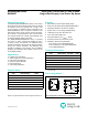
Figure 1a. Minimizing Offset Error Due to Input Bias Current
(Noninverting)
Figure 1b. Minimizing Offset Error Due to Input Bias Current
(Inverting)
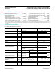
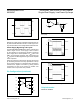
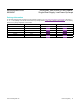
PIN
NAME FUNCTION
MAX4245 MAX4246 MAX4247
1 — — IN+ Noninverting Input
2 4 4 V
SS
Ground or Negative Supply
3 — — IN- Inverting Input
4 — — OUT Amplier Output
5 — —
SHDN
Shutdown
6 8 10 V
DD
Positive Supply
— 1 1 OUTA Amplier Output Channel A
— 2 2 INA- Inverting Input Channel A
— 3 3 INA+ Noninverting Input Channel A
— 5 7 INB+ Noninverting Input Channel B
— 6 8 INB- Inverting Input Channel B
— 7 9 OUTB Amplier Output Channel B
— — 5
SHDNA
Shutdown Channel A
— — 6
SHDNB
Shutdown Channel B
IN
R3
R3 = R1
║R2
R1 R2
V
DD
IN
R3
R3 = R1
║
R2
R1 R2
V
DD
MAX4245/MAX4246/
MAX4247
Ultra-Small, Rail-to-Rail I/O with Disable,
Single-/Dual-Supply, Low-Power Op Amps
www.maximintegrated.com
Maxim Integrated
│
7
Pin Description