
Datasheet


Power-Supply Voltage (V
DD
to V
SS
) ....................... -0.3V to +6V
All Other Pins ................................(V
SS
- 0.3V) to (V
DD
+ 0.3V)
Output Short-Circuit Duration
(OUT shorted to V
SS
or V
DD
) .............................. Continuous
Continuous Power Dissipation (T
A
= +70°C)
6-Pin SC70 (derate 3.1mW/°C above +70°C) .............245mW
6-Pin SOT23 (derate 8.7mW/°C above +70°C) ..........695mW
8-Pin SO (derate 5.9mW/°C above +70°C) ................. 471mW
8-Pin SOT23 (derate 9.1mW/°C above +70°C) ..........727mW
8-Pin µMAX (derate 4.5mW/°C above +70°C) ............362mW
10-Pin µMAX (derate 5.6mW/°C above +70°C) ..........444mW
Operating Temperature Range ......................... -40°C to +125°C
Junction Temperature ...................................................... +150°C
Storage Temperature Range ............................ -65°C to +160°C
Lead Temperature (soldering, 10s) .................................+300°C
Soldering Temperature (reflow) .......................................+260°C
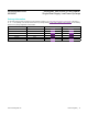
(V
DD
= +2.7V, V
SS
= 0V, V
CM
= 0V, V
OUT
= V
DD
/2, R
L
connected from OUT to V
DD
/ 2, SHDN_ = V
DD
(MAX4245/MAX4247 only),
T
A
= +25°C, unless otherwise noted.) (Note 1)
PARAMETER SYMBOL CONDITIONS MIN TYP MAX UNITS
Supply Voltage Range V
DD
Inferred from PSRR test 2.5 5.5 V
Supply Current (Per Amplier) I
DD
V
DD
= +2.7V 320 650
µA
V
DD
= +5.5V 375 700
Supply Current in Shutdown I
SHDN_
SHDN_ = V
SS
(Note 2) 0.05 0.5 µA
Input Offset Voltage V
OS
V
SS
- 0.1V ≤ V
CM
≤ V
DD
+ 0.1V ±0.4 ±1.5 mV
Input Bias Current I
B
V
SS
- 0.1V ≤ V
CM
≤ V
DD
+ 0.1V ±10 ±50 nA
Input Offset Current I
OS
V
SS
- 0.1V ≤ V
CM
≤ V
DD
+ 0.1V ±1 ±6 nA
Input Resistance R
IN
|V
IN+
- V
IN-
| ≤ 10mV 4000 kΩ
Input Common-Mode Voltage
Range
V
CM
Inferred from CMRR test V
SS
- 0.1 V
DD
+ 0.1 V
Common-Mode Rejection Ratio CMRR V
SS
- 0.1V ≤ V
CM
≤ V
DD
+ 0.1V 65 80 dB
Power-Supply Rejection Ratio PSRR 2.5V ≤ V
DD
≤ 5.5V 75 90 dB
Large-Signal Voltage Gain A
V
V
SS
+ 0.05V ≤ V
OUT
≤ V
DD
- 0.05V,
R
L
= 100kΩ
120
dB
V
SS
+ 0.2V ≤ V
OUT
≤ V
DD
- 0.2V,
R
L
= 2kΩ
95 110
Output Voltage Swing High V
OH
Specied as
V
DD
- V
OUT
R
L
= 100kΩ 1
mV
R
L
= 2kΩ 35 60
Output Voltage Swing Low V
OL
Specied as
V
OUT
- V
SS
R
L
= 100kΩ 1
mV
R
L
= 2kΩ 30 60
Output Short-Circuit Current I
OUT(SC)
V
DD
= +5.0V
Sourcing 11
mA
Sinking 30
Output Leakage Current in
Shutdown
I
OUT(SH)
Device in Shutdown Mode
(SHDN_ = V
SS
), V
SS
≤ V
OUT
≤ V
DD
(Note 2)
±0.01 ±0.5 µA
SHDN_ Logic Low V
IL
(Note 2) 0.3 x V
DD
V
SHDN_ Logic High V
IH
(Note 2) 0.7 x V
DD
V
SHDN_ Input Current I
L
/I
H
V
SS
≤ SHDN_ ≤ V
DD
(Note 2) 0.5 50 nA
MAX4245/MAX4246/
MAX4247
Ultra-Small, Rail-to-Rail I/O with Disable,
Single-/Dual-Supply, Low-Power Op Amps
www.maximintegrated.com
Maxim Integrated
│
2
Absolute Maximum Ratings
Stresses beyond those listed under “Absolute Maximum Ratings” may cause permanent damage to the device. These are stress ratings only, and functional operation of the device at these
or any other conditions beyond those indicated in the operational sections of the specifications is not implied. Exposure to absolute maximum rating conditions for extended periods may affect
device reliability.
Electrical Characteristics