
Datasheet


MAX3984
1Gbps to 10Gbps Preemphasis Driver with
Receive Equalizer
10 ______________________________________________________________________________________
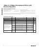
Pin Description
PIN NAME FUNCTION
1 V
CC1
Power-Supply Connection for Inputs. Connect to +3.3V.
2 IN+ Positive Data Input, CML. This input is internally terminated with 50.
3 IN- Negative Data Input, CML. This input is internally terminated with 50.
4, 8, 9, 16 GND Circuit Ground
5 OUT_LEV
Output-Swing Control Input, LVTTL with 20k Internal Pullup. Set to TTL high or open for maximum
output swing, or set to TTL low for reduced swing.
6 PE1
Output Preemphasis Control Input, LVTTL with 10k Internal Pullup. This pin is the most significant
bit of the 2-bit preemphasis control. Set high or open to assert this pin.
7 PE0
Output Preemphasis Control Input, LVTTL with 10k Internal Pullup. This pin is the least significant
bit of the 2-bit preemphasis control. Set high or open to assert this pin.
10 OUT- Negative Data Output, CML. This output is terminated with 50 to V
CC2
.
11 OUT+ Positive Data Output, CML. This output is terminated with 50 to V
CC2
.
12 V
CC2
Power-Supply Connection for Output. Connect to +3.3V.
13 TX_DISABLE
Transmitter Disable Input, LVTTL with 10k Internal Pullup. When high or open, differential output is
less than 10mV
P-P
. Set low for normal operation.
14 LOS
Loss-of-Signal Detect, Open-Collector TTL Output. Requires an external pullup 4.7k (+5.5V
maximum). This output sinks current when the input signal is above the LOS deassert level. To
disable squelch pull LOS to ground.
15 IN_LEV
Receive Equalization Control Input, LVTTL 40k Internal Pullup. Set to TTL high or open for higher
LOS assert/deassert levels and 10in FR-4 compensation. Set to TTL low for lower LOS assert/deassert
levels and to bypass the FR-4 equalization.
— EP
Exposed Pad. For optimal thermal conductivity, this pad must be soldered to the circuit board
ground.
Detailed Description
The MAX3984 is composed of a receiver, a driver, and
an LOS detector with selectable threshold. Equalization
is provided in the receiver. Selectable preemphasis
and selectable output amplitude are included in the
transmitter. The MAX3984 also includes transmit dis-
able control for the output.
Receiver
Data is fed into the MAX3984 through a CML input stage
and a selectable equalization stage. The fixed equalizer
in the receiver corrects for up to 10in of PCB loss on
FR-4 material at 10Gbps. The fixed equalizer can be
bypassed by setting the IN_LEV pin to a logic-low.
Driver
The driver includes four-state preemphasis to compen-
sate for up to 10m of 24 AWG, 100Ω balanced cable,
or 30in of FR-4. The OUT_LEV pin selects the output
amplitude. When OUT_LEV is low, the peak-to-peak
amplitude is 1000mV
P-P
. When OUT_LEV is high, the
peak-to-peak amplitude is 1200mV
P-P
.
Loss of Signal (LOS)
Input LOS detection is provided. This is an open-collec-
tor output and requires an external pullup resistor
(≥ 4.7kΩ). The pullup resistors should be connected
from LOS to a supply in the +3.0V to +5.5V range. The
LOS output is not valid until power-up is complete.