
Datasheet


MAX3980
3.125Gbps XAUI Quad Equalizer
_______________________________________________________________________________________ 3
ELECTRICAL CHARACTERISTICS (continued)
(V
CC
= +3.0V to +3.6V, input data rate = 3.125Gbps, T
A
= 0°C to +85°C. Typical values are at V
CC
= +3.3V and T
A
= +25°C, unless
otherwise noted.)
PARAMETER SYMBOL CONDITIONS MIN TYP MAX UNITS
TTL CONTROL PINS
Input High Voltage 2.0 V
Input Low Voltage 0.8 V
Input High Current 250 μA
Input Low Current 500 μA
Output High Voltage Internal 10kΩ pullup 2.4 V
Output Low Voltage Internal 10kΩ pullup 0.4 V
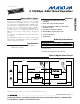
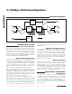
Note 1: K28.7 pattern is applied differentially at point A as shown in Figure 1.
Note 2: Total jitter does not include the signal source jitter. Total jitter (TJ) = [14.1 x RJ + DJ] where RJ is random RMS jitter and DJ
is maximum deterministic jitter. Signal source is a K28.5± pattern (00 1111 1010 11 0000 0101) for the deterministic jitter
test and K28.7 (0011111000) or equivalent for the random jitter test. Residual jitter is that which remains after equalizing
media-induced losses of the environment of Figure 1 or its equivalent. The deterministic jitter at point B must be from media-
induced loss and not from clock-source modulation. Jitter is measured at 0 at point C of Figure 1.
Note 3: Using K28.7 (0011111000) pattern.
OUTIN
SMA
CONNECTOR
SMA
CONNECTOR
≤ 40in (1m)
FR-4 STRIPLINE
A
B
C
MAX3980
Figure 1. Test Conditions Referenced in the Electrical Characteristics Table