
Datasheet


use information about the effects of temperature and
aging. The laser driver automatically adjusts the bias to
maintain the constant average power. The new bias con-
dition requires proper compensation of the modulation
current. The designer must predict the slope efficiency of
the laser after its bias threshold current has changed.
The modulation and bias currents under a single operat-
ing condition:
For AC-coupled diodes:
The required compensation factor is then:
Once the value of the compensation factor is known, the
fixed portion of the modulation current is calculated from:
Current Limits
To allow larger modulation current, the laser is AC-
coupled to the MAX3863. In this configuration, a con-
stant current is supplied from the inductor L
P
. When the
MOD pin is conducting, half of I
MOD
is supplied from
L
P
and half is from the laser diode. When MOD is off,
the current from the inductor flows to the bias input.
This reduces the current through the laser diode from
the average of I
BIAS
by half of I
MOD
. The resulting
peak-to-peak current through the laser diode is then
I
MOD
. See the
Typical Operating Circuit
. The require-
ment for compliance in the AC-coupled circuit:
•V
D
—Diode bias point voltage (1.2V typ)
•R
L
—Diode bias point resistance (5Ω typ)
• L—Diode lead inductance (1nH typ)
•R
D
—Series matching resistor (20Ω typ)
The time constant associated with the output pullup
inductor and the AC-coupling capacitor, impacts the
pattern-dependent jitter. For this second-order network
L
P
usually limits the low-frequency cutoff. The capacitor
C
D
is selected so:
Keep the peak voltage droop less than 3% of the peak-
to-peak amplitude during the maximum CID period t.
The required time constant:
If τ = L
P
/25Ω, and t = 100UI = 40ns, then L
P
= 35µH.
Place a good high-frequency inductor of 2µH on the
transmission line to the laser. Then you can place a
low-frequency inductor of 33µH at a convenient dis-
tance from the driver output.
Programming the Bias Current
When the APC loop is enabled, the actual bias current is
reduced from the maximum value to maintain constant
current from the monitor diode. With closed-loop control,
the bias current will be set by the transfer function of the
monitor diode to laser diode current. For example, if the
transfer function to the monitor diode is 10.0µA/mA, then
setting I
MD
for 500µA results in I
BIAS
equal to 50mA.
The bias current must be limited in case the APC loop
becomes open. The bias current also needs a set point
in case the APC control is not used. The BIASMAX pin
sets the maximum bias current. The BIASMAX current is
established by an internal current regulator, which main-
tains the bandgap voltage of 1.2V across the external
28 1
35
.%=
=×
−
−
e
t
t
τ
τ
CRR
L
RR
DDL
P
DL
×+>
+
()
()
V
I
RR V
CC
MOD
DL
−
×+≥
2
18().
IIKI
MODS MOD BIAS
=×−
K
II
II
MOD MOD
BIAS BIAS
=
−
−
21
21
II
I
BIAS TH
MOD
=+
2
I
P
r
r
MOD
AVG
e
e
=× ×
+
−
2
1
1
η
MAX3863
2.7Gbps Laser Driver with Modulation
Compensation
_______________________________________________________________________________________ 9
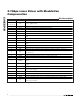
PARAMETER SYMBOL RELATION
Average Power P
AVG
P
AVG
= (P
0
+ P
1
)/2
Extinction Ratio r
e
r
e
= P
1
/P
0
Optical Power of a 1 P
1
P
1
= 2P
AVG
r
e
/(r
e
+ 1)
Optical Power of a Zero P
0
P
0
= 2P
AVG
/(r
e
+ 1)
Optical Amplitude P
P-P
P
P-P
= P
1
-
P
0
Laser Slope Efficiency ηη = P
P-P
/I
MOD
Modulation Current I
MOD
I
MOD
= P
P-P
/η
Threshold Current I
TH
P
0
at I ≥ I
TH
Bias Current I
BIAS
I
BIAS
≥ I
TH
+ I
MOD
/2
Laser to Monitor
Transfer
ρ
MON
I
MD
/P
AVG
Table 1. Optical Power Relations