
Datasheet

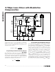

MAX3863
2.7Gbps Laser Driver with Modulation
Compensation
6 _______________________________________________________________________________________
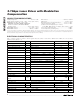
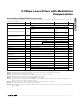
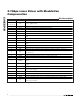
Pin Description
PIN NAME FUNCTION
1, 4, 5, 8,
14, 19, 22, 27
V
CC
Positive Supply Voltage
2 DATA+ Data Input, with On-Chip Termination
3 DATA- Complementary Data Input, with On-Chip Termination
6 CLK+ Clock Input for Data Retiming, with On-Chip Termination
7 CLK- Complementary Clock Input for Data Retiming, with On-Chip Termination
9 APCSET Monitor Diode Current Set Point
10 APCFILT1
APC Loop Filter Capacitor. Short to ground to disable the correction loop through the monitor
diode.
11 APCFILT2 APC Loop Filter Capacitor
12 PWC+ Input for Modulation Pulse-Width Adjustment. Connected to GND through R
PWC
.
13 PWC-
Complementary Input for Modulation Pulse-Width Adjustment. Connected to GND through
R
PWC
.
15 MK+ Voltage Proportional to the Mark Density. MK+ = MK- for 50% duty cycle.
16 MK- Voltage Inversely Proportional to the Mark Density
17 FAIL Alarm for Shorts on Current Set Pins and APC Loop Failure Conditions, Active Low
18 BIAS
Laser Diode Bias Current Source (Sink Type) to Bias the Laser Diode. Connect to the laser
with an inductor.
20 MOD Driver Output. AC-coupled to the laser diode.
21 MODN Complementary Driver Output. Connect to dummy load off-chip.
23 MD Monitor Diode Connection
24 MDMON
Monitor for MD Current. Voltage developed across an external resistor from mirrored MD
current.
25 MODMON
Monitor for Modulation Current. Voltage developed from I
MOD
mirrored through an external
resistor.
26 BIASMON Monitor for Bias Current. Voltage developed from I
BIAS
mirrored through an external resistor.
28 MODCOMP
Couples the Bias Current to the Modulation Current. Mirrors I
BIAS
through an external resistor.
Open for zero coupling.
29 MODSET External Resi stor to Program I
MODC
(I
MOD
= I
MODS
+ I
MODC
)
30 BIASMAX External Resistor to Program the Maximum I
BIAS
31 EN Modulation and Bias Current Enable, Active Low. Current disabled when floating or high.
32 RTEN Data Retiming Enable Input, Active Low. Retiming disabled when floating or high.
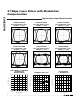
—
EP
Exposed Pad. The exposed pad must be soldered to circuit-board ground for proper thermal
and electrical operation.