
Datasheet


MAX3863
2.7Gbps Laser Driver with Modulation
Compensation
_______________________________________________________________________________________ 3
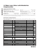
ELECTRICAL CHARACTERISTICS (continued)
(V
CC
= +3.15V to +3.6V, T
A
= -40°C to +85°C. Typical values are at V
CC
= +3.3V, I
BIAS
= 50mA, I
MOD
= 40mA, T
A
= +25°C, unless
otherwise noted.) (Notes 1, 9)
Note 1: Specifications at -40°C are guaranteed by design and characterization.
Note 2: Excluding I
BIAS
, I
MOD
, I
BIASMON
, I
MODMON
, I
FAIL
, and I
PWC
. Input clock and data are AC-coupled.
Note 3: Guaranteed by design and characterization.
Note 4: An external capacitor at APCFILT1 and APCFILT2 is used to set the time constant.
Note 5: For both data inputs DATA+, DATA- and clock inputs CLK+, CLK-.
Note 6: Measured using a 2.7Gbps repeating 0000 0000 1111 1111 pattern.
Note 7: For pulse width, PW = 100%: Rp = Rn = 500Ω (or open) or PWC+ = PWC- ≈ +0.5V. For PW > 100%: Rp > Rn or PWC+ >
PWC-. For PW < 100%: Rp < Rn or PWC+ < PWC-.
Note 8: Measured using a 2
13
- 1 PRBS with 80 zeros + 80 ones input data pattern or equivalent.
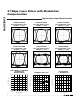
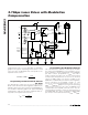
Note 9: AC characterization performed using the circuit in Figure 1.
Note 10: Power-Supply Noise Rejection (PSNR) = 20log
10
(V
NOISE (on VCC)
/ΔV
OUT
). V
OUT
is the voltage across the 25Ω load when no
input is applied.
PARAMETER SYMBOL CONDITIONS MIN TYP MAX UNITS
At high V
CC
Single-Ended Input (DC-Coupled) V
IS
At low V
C C
- 1.0 V
C C
- 0.1
V
At high
V
CC
+
0.05
V
CC
+
0.4
Single-Ended Input (AC-Coupled) V
IS
At low
V
C C
-
0.4
V
C C
-
0.05
V
DC-coupled 0.2 2.0
Differential Input Swing V
ID
AC-coupled 0.2 1.6
V
P-P
Input Data Rate NRZ (Note 3) 3.2 Gbps
f ≤ 2.7GHz 17
Input Return Loss RL
IN
(Notes 3, 5)
2.7GHz < f ≤ 4GHz 14
dB
Turn-Off Delay from EN EN = high (Note 3) 1.0 µs
Setup Time t
SU
Figure 2 (Note 3) 90 ps
Hold Time t
HD
Figure 2 (Note 3) 90 ps
Pulse-Width Adjustment Range Z
L
= 25Ω (Notes 3, 6) ±185 ±220 ps
Pulse-Width Stability PWC+ and PWC- open (Notes 3, 6) ±18.5 ps
Differential Pulse-Width Control
Input Range
For P WC + and P W C - ( N otes 3, 7) , V
C M
= 0.5V -1.0 1.0 V
Differential Mark Density 0% to 100%, V
MK
+ - V
MK
- ±0.85 V
Differential Mark-Density Voltage
to Mark-Density Ratio
15.5 V/%
Output Edge Speed t
R
, t
F
Z
L
= 25Ω (20% to 80%) (Notes 3, 6) 50 85 ps
Output Overshoot δ Z
L
= 25Ω (Note 3) ±7%
Random Jitter (Notes 3, 6) 0.8 1.3 ps
RMS
Data Rate = 2.7Gbps (Notes 3, 8) 8 40
Deterministic Jitter
Data Rate = 3.2Gbps (Notes 3, 8) 10 40
ps
P-P