
Datasheet


MAX3863
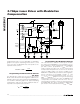
2.7Gbps Laser Driver with Modulation
Compensation
2 _______________________________________________________________________________________
ABSOLUTE MAXIMUM RATINGS
ELECTRICAL CHARACTERISTICS
(V
CC
= +3.15V to +3.6V, T
A
= -40°C to +85°C. Typical values are at V
CC
= +3.3V, I
BIAS
= 50mA, I
MOD
= 40mA, T
A
= +25°C, unless
otherwise noted.) (Notes 1, 9)
Stresses beyond those listed under “Absolute Maximum Ratings” may cause permanent damage to the device. These are stress ratings only, and functional
operation of the device at these or any other conditions beyond those indicated in the operational sections of the specifications is not implied. Exposure to
absolute maximum rating conditions for extended periods may affect device reliability.
Supply Voltage V
CC
...............................................-0.5V to +5.0V
DATA+, DATA- and CLK+, CLK- ....(V
CC
- 1.5V) to (V
CC
+ 0.5V)
RTEN, EN, BIAS, MK+, MK-, PWC+, PWC-
MODMON, BIASMON, MDMON, MODCOMP,
APCFILT1, APCFILT2, BIASMAX, MODSET,
APCSET Voltage ......................................-0.5V to (V
CC
+ 0.5V)
MOD, MODN Voltage .......................................0 to (V
CC
+ 1.5V)
MOD, MODN Current......................................-20mA to +150mA
BIAS Current ...................................................-20mA to +150mA
MD Current............................................................-5mA to +5mA
Operating Junction Temperature Range...........-55°C to +150°C
Storage Temperature Range .............................-55°C to +150°C
Continuous Power Dissipation (T
A
= +85°C)
32-Pin QFN, TQFN (derate 21.2mW/°C above +85°C)....1.3W
Processing Temperature (die) .........................................+400°C
Lead Temperature (soldering, 10s) ................................ +300°C
PARAMETER SYMBOL CONDITIONS MIN TYP MAX UNITS
Power-Supply Current I
CC
(Note 2) 58 85 mA
Power-Supply Noise Rejection PSNR f = 100kHz, 100mV
P-P
(Note 10) 40 dB
Power-Supply Threshold Output enabled 2.8 V
Single-Ended Input Resistance Input to V
CC
40 50 60 Ω
Bias-Current Setting Range 4 100 mA
APC open loop, I
BIAS
= 100mA, T
A
= +25°C -15 +15
Bias-Current Setting Error
APC open loop, I
BIAS
= 4mA, T
A
= +25°C -20 +20
%
Bias Off-Current EN high 0.1 mA
I
BIAS
to I
BIASMON
Ratio 34 40 46 mA/mA
APC open loop, 10mA ≤ I
BIAS
≤ 100mA (Note 3) -480 +480
Bias-Current Temperature Stability
APC open loop, 4mA
≤ I
BIAS
≤ 100mA (Note 3) ±390
ppm/°C
Modulation-Current Setting Range 7 80 mA
Modulation-Current Setting Error APC open loop, 25Ω load, T
A
= +25°C -15 +15 %
Modulation Off-Current EN high 0.1 mA
Modulation-Current Temperature
Stability
APC open loop (Note 3) -480 +480 ppm/°C
I
MOD
to I
MODMON
Ratio 38 46 53 mA/mA
Modulation Compensation Range K K = ΔI
MODC
/ΔI
BIAS
0 1.5 mA/mA
MD Pin Voltage 1.75 V
Monitor Photodiode Current
Range
I
MD
30 2000 µA
APC Loop Time Constant t
APC
(Notes 3, 4) 1 4 1000 µs
APC Open Loop 4mA ≤ I
BIAS
≤ 10mA (Note 3) ±390 mA
V
MDMON
to I
MD
Ratio R
MDMON
= 4kΩ 0.8 1.0 1.2 mV/µA
EN and RTEN Input High V
IH
2.0 V
EN and RTEN Input Low V
IL
0.8 V
FAIL Output High V
OH
Source 150µA 2.4 V
FAIL Output Low V
OL
Sink 2mA 0.4 V