
Datasheet
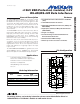


MAX3480EA/MAX3480EB
±15kV ESD-Protected, Isolated, 3.3V
RS-485/RS-422 Data Interfaces
_______________________________________________________________________________________ 7
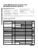
______________________________________________________________Pin Description
PIN NAME FUNCTION
PINS ON THE NONISOLATED SIDE
1V
CC1
Logic-Side (Nonisolated Side) +3.3V Supply Voltage Input. Connect to pins 2, 10, and 14.
2V
CC2
Logic-Side (Nonisolated Side) +3.3V Supply Voltage Input. Connect to pins 1, 10, and 14.
3, 4 D1, D2 Boost-Voltage Generator Outputs. See Figures 1 and 2.
5, 12
GND1,
GND2
Logic-Side Ground Inputs. Must be connected; not internally connected.
6FS
Frequency Switch Input. If V
FS
= V
CC
, switch frequency is high; if FS = 0, switch frequency is low
(normal connection).
7SDPower-Supply Shutdown Input. Must be connected to logic ground.
8V
CC3
Boosted V+ Voltage Input. Must be connected as shown in Figures 1 and 2.
9DI
Driver Input. With DE´ high, a low on DI´ forces output A low and output B high. Similarly, a high on
DI´ forces output A high and output B low. Drives internal LED cathode through R1 (Table 1).
10 V
CC4
Logic-Side (Nonisolated Side) +3.3V Supply Voltage Input. Connect to pins 1, 2, and 14.
11 DE
Driver-Enable Input. The driver outputs, A and B, are enabled by bringing DE´ high. The driver
outputs are high impedance when DE´ is low. If the driver outputs are enabled, the device functions
as a line driver. While the driver outputs are high impedance, the device functions as a line receiver.
Drives internal LED cathode through R2 (Table 1).
13 RO
Receiver Output. If A > B by 200mV, RO is low; if A < B by 200mV, RO is high. Open collector; must
have pullup (R3) to V
CC
(Table 1).
14 V
CC5
Logic-Side (Nonisolated Side) +3.3V Supply Voltage Input. Connect to pins 1, 2, and 10.