
Datasheet


MAX3480EA/MAX3480EB
±15kV ESD-Protected, Isolated, 3.3V
RS-485/RS-422 Data Interfaces
2 _______________________________________________________________________________________
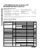
ABSOLUTE MAXIMUM RATINGS
ELECTRICAL CHARACTERISTICS
(V
CC
= V
CC1
= V
CC2
= V
CC4
= V
CC5
= +3.0V to +3.6V, FS = 0, T
A
= T
MIN
to T
MAX
, unless otherwise noted. Typical values are at V
CC
=
+3.3V and T
A
= +25°C.) (Notes 1, 2)
Stresses beyond those listed under “Absolute Maximum Ratings” may cause permanent damage to the device. These are stress ratings only, and functional
operation of the device at these or any other conditions beyond those indicated in the operational sections of the specifications is not implied. Exposure to
absolute maximum rating conditions for extended periods may affect device reliability.
With Respect to GND
Supply Voltage (V
CC
1,
V
CC
2,
V
CC
4,
V
CC
5
) .......-0.3V to +3.8V
Supply Voltage (V
CC3
) ........................................-0.3V to +7V
Control Input Voltage (SD, FS) ............-0.3V to (V
CC3
+ 0.3V)
Receiver Output Voltage (RO).............-0.3V to (V
CC5
+ 0.3V)
With Respect to ISO COM
Control Input Voltage (ISO DE _)......-0.3V to (ISO V
CC_
+ 0.3V)
Driver Input Voltage (ISO DI _) .....-0.3V to (ISO V
CC_
+ 0.3V)
Receiver Output Voltage (ISO RO _) ..-0.3V to (ISO V
CC_
+ 0.3V)
Driver Output Voltage (A, B)..............................-8V to +12.5V
Receiver Input Voltage (A, B)............................-8V to +12.5V
LED Forward Current (DI, DE, ISO RO LED) ......................50mA
Continuous Power Dissipation (T
A
= +70°C)
28-Pin PDIP (derate 9.09mW/°C above +70°C)............727mW
Operating Temperature Ranges
MAX3480E_CPI..................................................0°C to +70°C
MAX3480E_EPI...............................................-40°C to +85°C
Storage Temperature Range .............................-65°C to +150°C
Lead Temperature (soldering, 10s) .................................+300°C
PARAMETER
SYMBOL
CONDITIONS
MIN TYP MAX
UNITS
f
SWL
FS = 0 60
Switch Frequency
f
SWH
FS = V
CC
or open
900
kHz
R
L
= ∞
130 250
MAX3480EA,
DE´ = V
CC
or open
R
L
= 54Ω
220
R
L
= ∞ 80
200
Operating Supply Current I
CC
MAX3480EB,
DE´ = V
CC
or open
R
L
= 54Ω
180
mA
Shutdown Supply Current (Note 3)
I
SHDN
SD = V
CC3
0.2 µA
V
FSH
High 2.4
FS Input Threshold
V
FSL
Low 0.8
V
FS Input Pullup Current I
FSL
FS low 50 µA
FS Input Leakage Current I
FSM
FS high 10 pA
Input High Voltage V
IH
DE´, DI´, Figure 1 V
CC
- 0.4 V
Input Low Voltage V
IL
DE´, DI´, Figure 1 0.4 V
Isolation Voltage V
ISO
T
A
= +25°C, 1min (Note 4)
1260
V
RMS
V
SDH
High 2.4 1
Shutdown Input Threshold
V
SDL
Low 1 0.8
V
Isolation Resistance R
ISO
T
A
= +25°C, V
ISO
= ±50VDC
100 10,000
MΩ
Isolation Capacitance C
ISO
f = 1MHz 10 pF
ESD Protection ESD
A, B, Y, and Z pins, tested at Human Body
Model
±15
kV
Differential Driver Output
(No Load)
V
OD1
8V
R = 50Ω (RS-422) 2
Differential Driver Output V
OD2
R = 27Ω (RS-485), Figure 3 1.5 5.0
V
Differential 0.3
Change in Magnitude of Driver
Output Voltage for Complementary
Output States
∆V
OD
R = 27Ω or 50Ω,
Figure 3
Common mode 0.3
V